Reset Generation Module (MC_RGM) RM0046
192/936 Doc ID 16912 Rev 5
8.3.1 Register Descriptions
Unless otherwise noted, all registers may be accessed as 32-bit words, 16-bit half-words, or
8-bit bytes. The bytes are ordered according to big endian. For example, the
RGM_DES[8:15] register bits may be accessed as a word at address 0xC3FE_4000, as a
half-word at address 0xC3FE_4002, or as a byte at address 0xC3FE_4004.
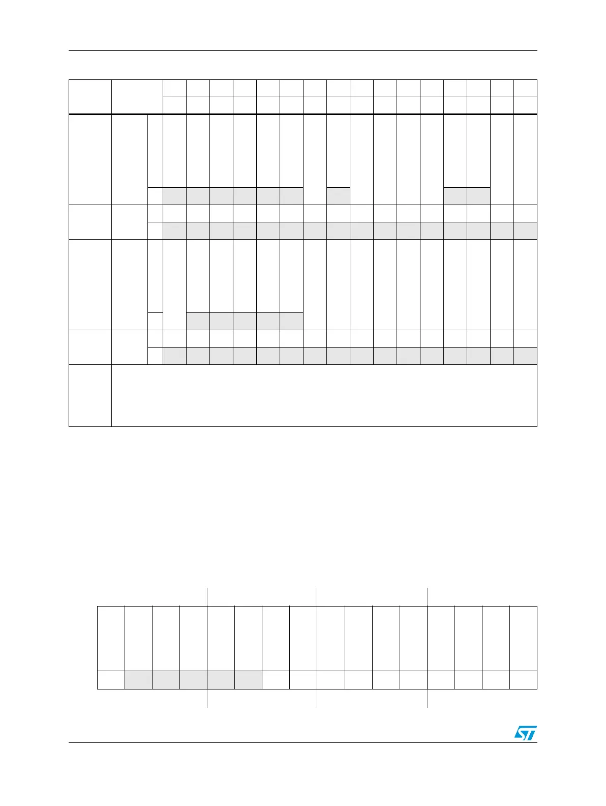
Functional Event Status Register (RGM_FES)
0xC3FE
_4018
RGM_
FESS
R
SS_EXR
00000
SS_PLL1
SS_FLASH
SS_LVD45
SS_CMU0_FHL
SS_CMU0_OLR
SS_PLL0
SS_CHKSTOP
SS_SOFT
SS_CORE
SS_JTAG
W
R0000000000000000
W
0xC3FE
_401C
RGM_
FBRE
R
BE_EXR
00000
BE_PLL1
BE_FLASH
BE_LVD45
BE_CMU0_FHL
BE_CMU0_OLR
BE_PLL0
BE_CHKSTOP
BE_SOFT
BE_CORE
BE_JTAG
W
R0000000000000000
W
0xC3FE
_4020
…
0xC3FE
_7FFC
reserved
Table 57. MC_RGM Memory Map (continued)
Address Name
01232756789101112131415
16 17 18 19 20 21 22 23 24 25 26 27 28 29 30 31
Figure 69. Functional Event Status Register (RGM_FES)
Address 0xC3FE_4000 Access: User read, Supervisor read/write, Test read/write
0123456789101112131415
R
F_EXR
00000
F_PLL1
F_FLASH
F_LVD45
F_CMU0_FHL
F_CMU0_OLR
F_PLL0
F_CHKSTOP
F_SOFT
F_CORE
F_JTAG
Ww1c w1c w1c w1c w1c w1c w1c w1c w1c w1c w1c
POR0000000000000000