Clock Description RM0046
102/936 Doc ID 16912 Rev 5
4.8.5 Register description
The PLL operation is controlled by two registers. Those registers can only be written in
supervisor mode.
Control Register (CR)
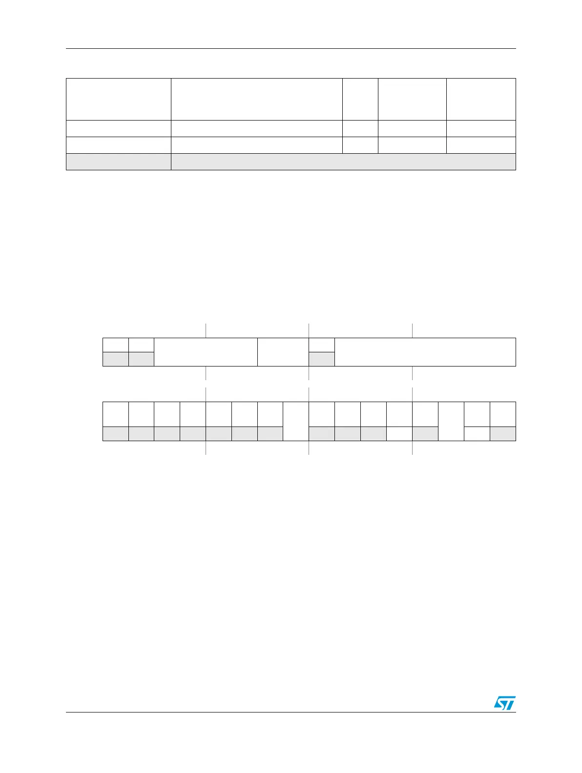
Table 12. FMPLL memory map
Offset from
ME_CGM_BASE
(1)
FMPLL_0: 0xC3FE_00A0
Register
Access
Reset value Location
0x0000 CR—Control Register R/W 0x0080_0000 on page 4-102
0x0004 MR—Modulation register R/W 0x0080_0000 on page 4-104
0x0004–0x000F Reserved
1. FMPLL_x are mapped through the ME_CGM Register Slot
Figure 15. Control Register (CR)
Address:
Base + 0x0000
FMPLL_0 = 0xC3FE_00A0
Access: Supervisor read/write
User read-only
0123456789101112131415
R 0 0
IDF[3:0] ODF[1:0]
0
NDIV[6:0]
W
Reset0000010101000000
16 17 18 19 20 21 22 23 24 25 26 27 28 29 30 31
R
0000000
en_pll
_sw
0
unlock
_once
0i_lock
s_lock
pll_fail
_mask
pll_fai
l_flag
1
W w1c w1c
Reset0000000000000001