RM0046 Deserial Serial Peripheral Interface (DSPI)
Doc ID 16912 Rev 5 475/936
When the CONT = 1 and the CS signal for the next transfer is the same as for the current
transfer, the CS signal remains asserted for the duration of the two transfers. The delay
between transfers (t
DT
) is not inserted between the transfers.
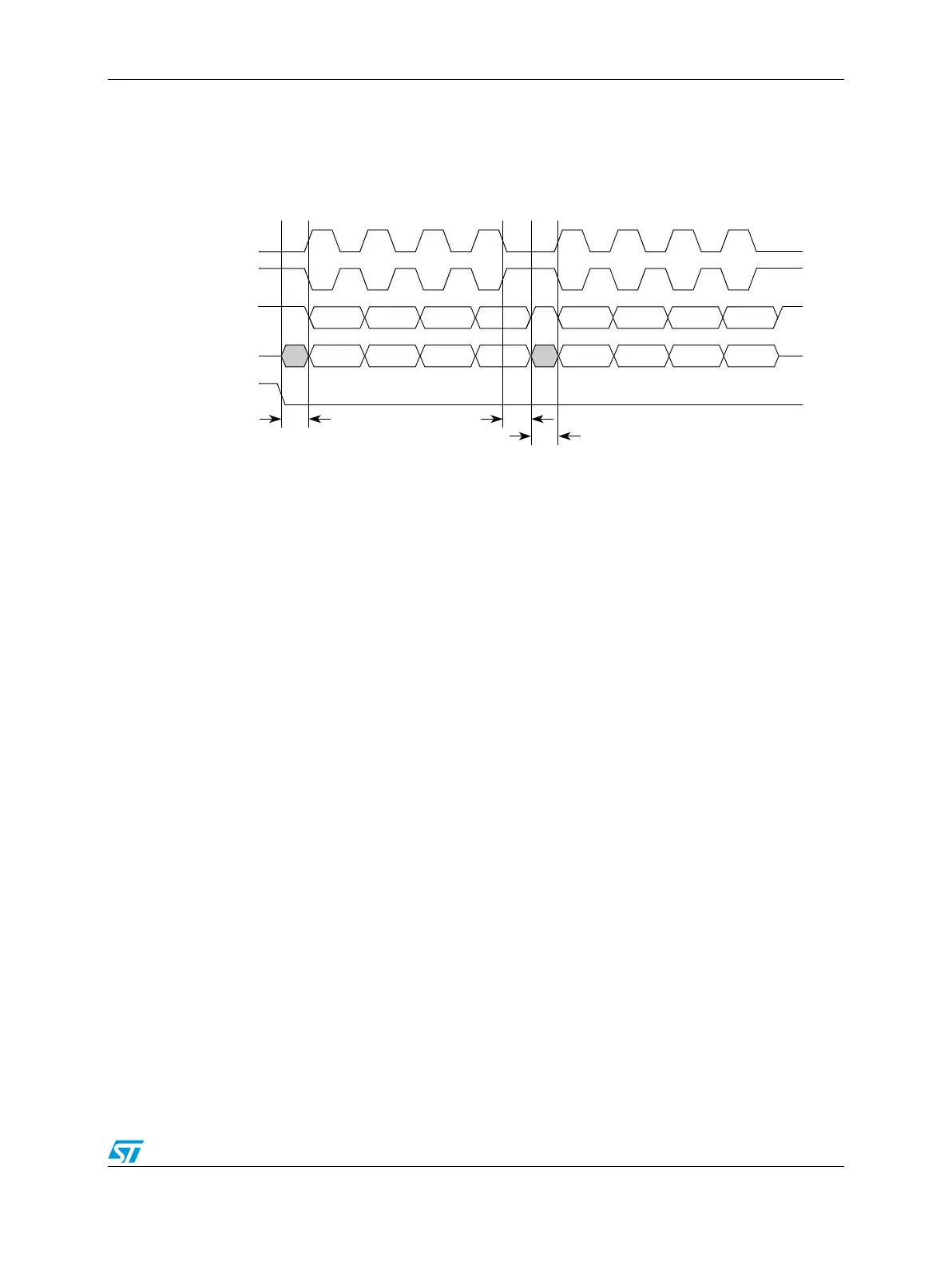
Figure 225 shows the timing diagram for two 4-bit transfers with CPHA = 1 and CONT = 1.
Figure 225. Example of continuous transfer (CPHA = 1, CONT = 1)
In Figure 225, the period length at the start of the next transfer is the sum of t
ASC
and t
CSC
;
i.e., it does not include a half-clock period. The default settings for these provide a total of
four system clocks. In many situations, t
ASC
and t
CSC
must be increased if a full half-clock
period is required.
Switching CTARs between frames while using continuous selection can cause errors in the
transfer. The CS signal must be negated before CTAR is switched.
When the CONT bit = 1 and the CS signals for the next transfer are different from the
present transfer, the CS signals behave as if the CONT bit was not set.
Note: It is mandatory to fill the TXFIFO with the number of entries that will be concatenated
together under one PCS assertion for both master and slave before the TXFIFO becomes
empty. For example; while transmitting in master mode, it should be ensured that the last
entry in the TXFIFO, after which TXFIFO becomes empty, must have the CONT bit in
command frame as deasserted (i.e. CONT bit = 0).While operating in slave mode, it should
be ensured that when the last-entry in the TXFIFO is completely transmited (i.e. the
corresponding TCF flag is asserted and TXFIFO is empty) the slave should be de-selected
for any further serial communication; else an underflow error occurs
Clock polarity switching between DSPI transfers
If it is desired to switch polarity between non-continuous DSPI frames, the edge generated
by the change in the idle state of the clock occurs one system clock before the assertion of
the chip select for the next frame.
Refer to Section , “DSPI Clock and Transfer Attributes Registers 0–7 (DSPIx_CTARn).
In Figure 226, time ‘A’ shows the one clock interval. Time ‘B’ is user programmable from a
minimum of two system clocks.
SCK
(CPOL = 0)
CS
t
ASC
SCK
(CPOL = 1)
Master SOUT
t
CSC
t
CSC
t
CSC
= CS to SCK delay.
t
ASC
= After SCK delay.
Master SIN