RM0046 Deserial Serial Peripheral Interface (DSPI)
Doc ID 16912 Rev 5 471/936
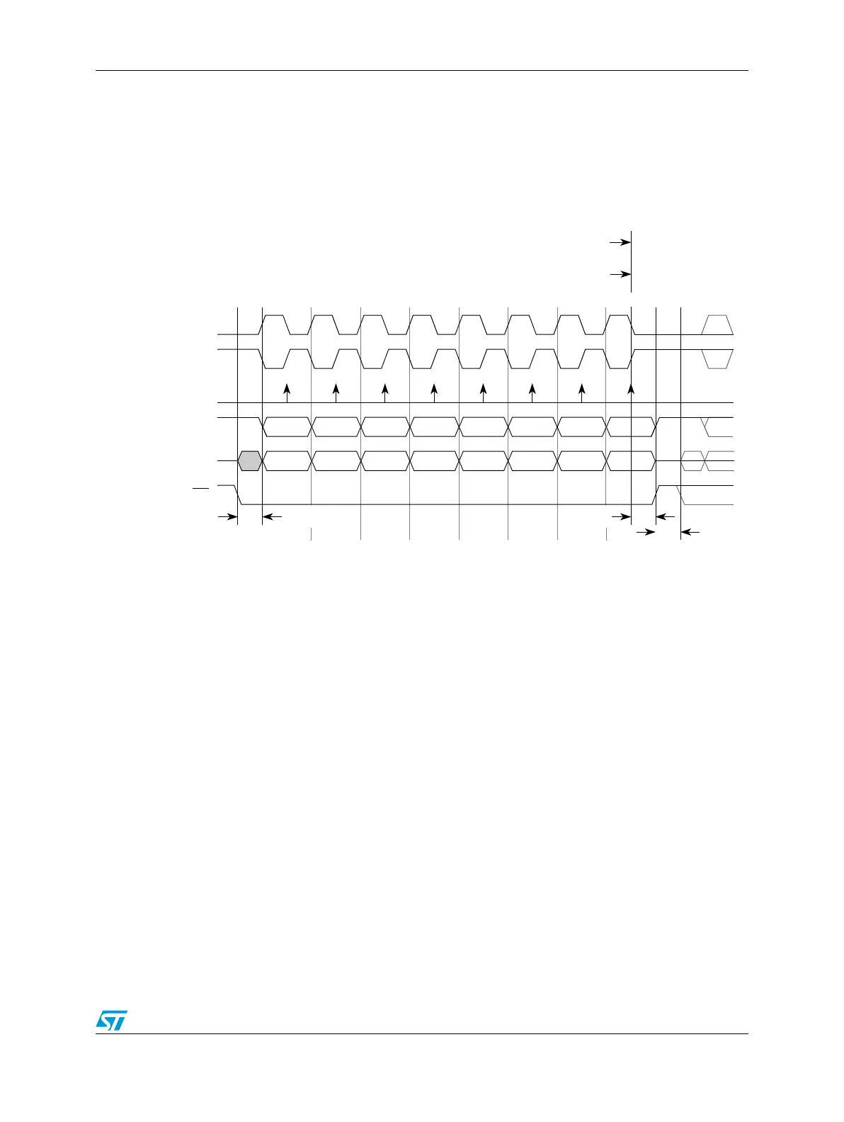
Classic SPI transfer format (CPHA = 1)
The transfer format shown in Figure 221 is used to communicate with peripheral SPI slave
devices that require the first SCK_x edge before the first data bit becomes available on the
slave SOUT_x pin. In this format the master and slave devices change the data on their
SOUT_x pins on the odd-numbered SCK_x edges and sample the data on their SIN_x pins
on the even-numbered SCK_x edges.
Figure 221. DSPI transfer timing diagram (MTFE = 0, CPHA = 1, FMSZ = 8)
The master initiates the transfer by asserting the CSx signal to the slave. After the
t
CSC
delay has elapsed, the master generates the first SCK_x edge and at the same time places
valid data on the master SOUT_x pin. The slave responds to the first SCK_x edge by
placing its first data bit on its slave SOUT_x pin.
At the second edge of the SCK_x the master and slave sample their SIN_x pins. For the rest
of the frame the master and the slave change the data on their SOUT_x pins on the odd-
numbered clock edges and sample their SIN_x pins on the even-numbered clock edges.
After the last clock edge occurs a delay of t
ASC
is inserted before the master negates the
CSx signal. A delay of t
DT
is inserted before a new frame transfer can be initiated by the
master.
For CPHA = 1 the master EOQF and TCF and slave TCF are set at the last serial clock
edge (edge 16) of Figure 221. For CPHA = 1 the master and slave RXCTR counters are
updated on the same clock edge.
Slave (CPHA = 1): TCF is set and RXCTR counter is updated at
last SCK edge of frame (edge 16)
SCK
123456789101112131415
(CPOL = 0)
PCSx / SS
t
ASC
SCK
(CPOL = 1)
Master and slave
sample
Master SOUT/
Slave SIN
Master SIN/
Slave SOUT
Bit 6
Bit 1
Bit 5
Bit 2
Bit 4
Bit 3
Bit 3
Bit 4
Bit 2
Bit 5
Bit 1
Bit 6
LSB
MSB
MSB
LSB
t
DT
t
CSC
MSB first (LSBFE = 0):
LSB first (LSBFE = 1):
t
CSC
= CS to SCK delay.
t
ASC
= After SCK delay.
t
DT
= Delay after transfer (minimum CS negation time).
Master (CPHA = 1): TCF and EOQF are set and RXCTR counter
is updated at last SCK edge of frame (edge 16)
16