Deserial Serial Peripheral Interface (DSPI) RM0046
442/936 Doc ID 16912 Rev 5
CS5 is not used in slave mode. On DSPI_0, this is CS7.
Serial Input (SIN_x)
SIN_x is a serial data input signal.
Serial Output (SOUT_x)
SOUT_x is a serial data output signal.
Serial Clock (SCK_x)
SCK_x is a serial communication clock signal. In master mode, the DSPI generates the
SCK. In slave mode, SCK_x is an input from an external bus master.
20.7 Memory map and registers description
20.7.1 Memory map
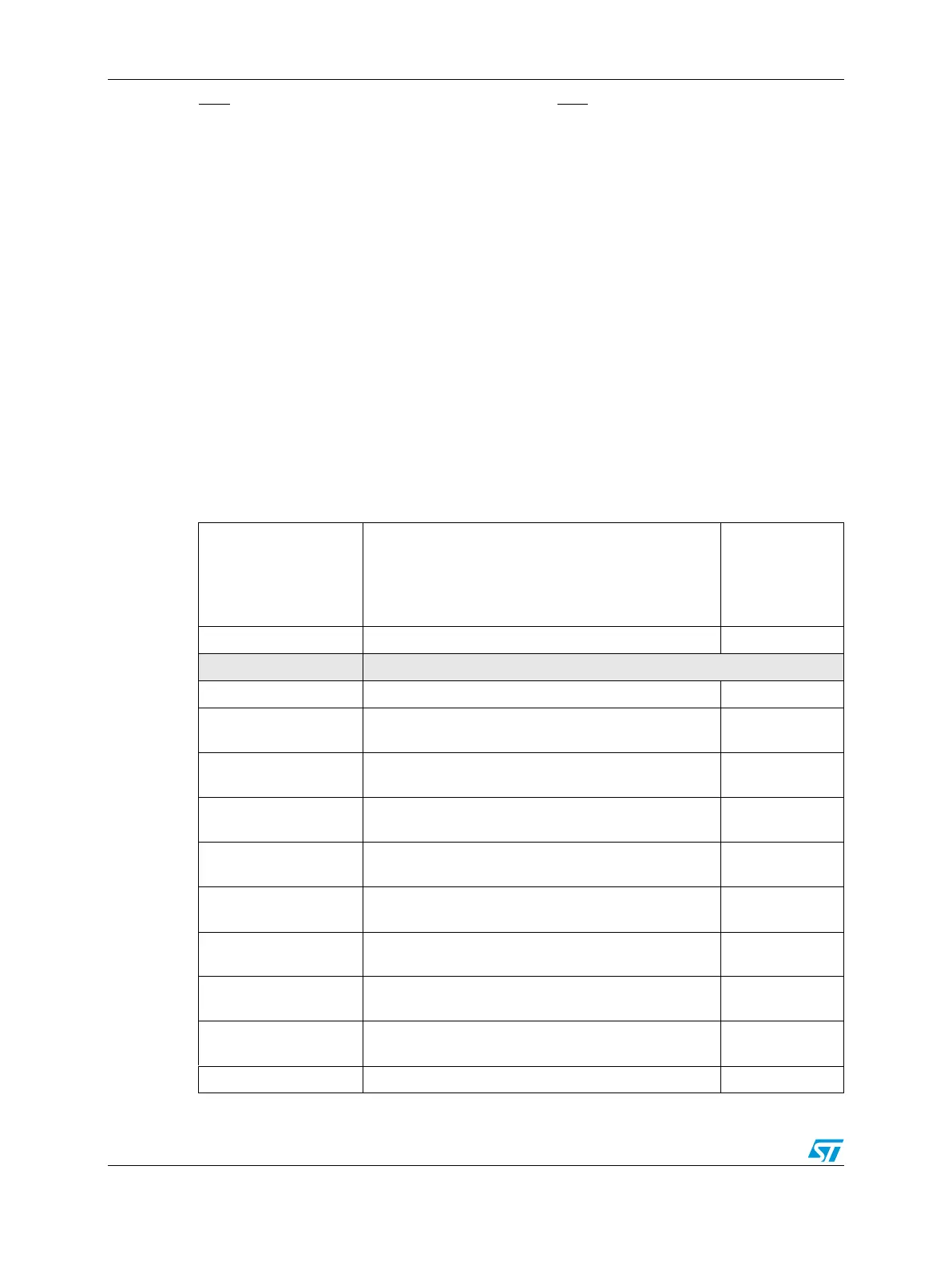
Table 205 shows the DSPI memory map.
Table 205. DSPI memory map
Offset from
DSPI_BASE
0xFFF9_0000 (DSPI_0)
0xFFF9_4000 (DSPI_1)
0xFFF9_8000 (DSPI_2)
Register Location
0x0000 DSPI_MCR—DSPI module configuration register on page 20-443
0x0004 Reserved
0x0008 DSPI_TCR—DSPI transfer count register on page 20-446
0x000C
DSPI_CTAR0—DSPI clock and transfer attributes
register 0
on page 20-447
0x0010
DSPI_CTAR1—DSPI clock and transfer attributes
register 1
on page 20-447
0x0014
DSPI_CTAR2—DSPI clock and transfer attributes
register 2
on page 20-447
0x0018
DSPI_CTAR3—DSPI clock and transfer attributes
register 3
on page 20-447
0x001C
DSPI_CTAR4—DSPI clock and transfer attributes
register 4
on page 20-447
0x0020
DSPI_CTAR5—DSPI clock and transfer attributes
register 5
on page 20-447
0x0024
DSPI_CTAR6—DSPI clock and transfer attributes
register 6
on page 20-447
0x0028
DSPI_CTAR7—DSPI clock and transfer attributes
register 7
on page 20-447
0x002C DSPI_SR—DSPI status register on page 20-453