IEEE 1149.1 Test Access Port Controller (JTAGC) RM0046
844/936 Doc ID 16912 Rev 5
35.7.1 Instruction register
The JTAGC uses a 5-bit instruction register as shown in Figure 498. The instruction register
allows instructions to be loaded into the module to select the test to be performed or the test
data register to be accessed or both. Instructions are shifted in through TDI while the TAP
controller is in the Shift-IR state, and latched on the falling edge of TCK in the Update-IR
state. The latched instruction value can only be changed in the update-IR and test-logic-
reset TAP controller states. Synchronous entry into the test-logic-reset state results in the
IDCODE instruction being loaded on the falling edge of TCK. Asynchronous entry into the
test-logic-reset state results in asynchronous loading of the IDCODE instruction. During the
capture-IR TAP controller state, the instruction shift register is loaded with the value
0b10101, making this value the register’s read value when the TAP controller is sequenced
into the Shift-IR state.
35.7.2 Bypass register
The bypass register is a single-bit shift register path selected for serial data transfer
between TDI and TDO when the BYPASS, CLAMP, HIGHZ or reserve instructions are
active. After entry into the capture-DR state, the single-bit shift register is set to a logic 0.
Therefore, the first bit shifted out after selecting the bypass register is always a logic 0.
35.7.3 Device identification register
The device identification register, shown in Figure 499, allows the part revision number,
design center, part identification number, and manufacturer identity code to be determined
through the TAP. The device identification register is selected for serial data transfer
between TDI and TDO when the IDCODE instruction is active. Entry into the capture-DR
state while the device identification register is selected loads the IDCODE into the shift
register to be shifted out on TDO in the Shift-DR state. No action occurs in the update-DR
state.
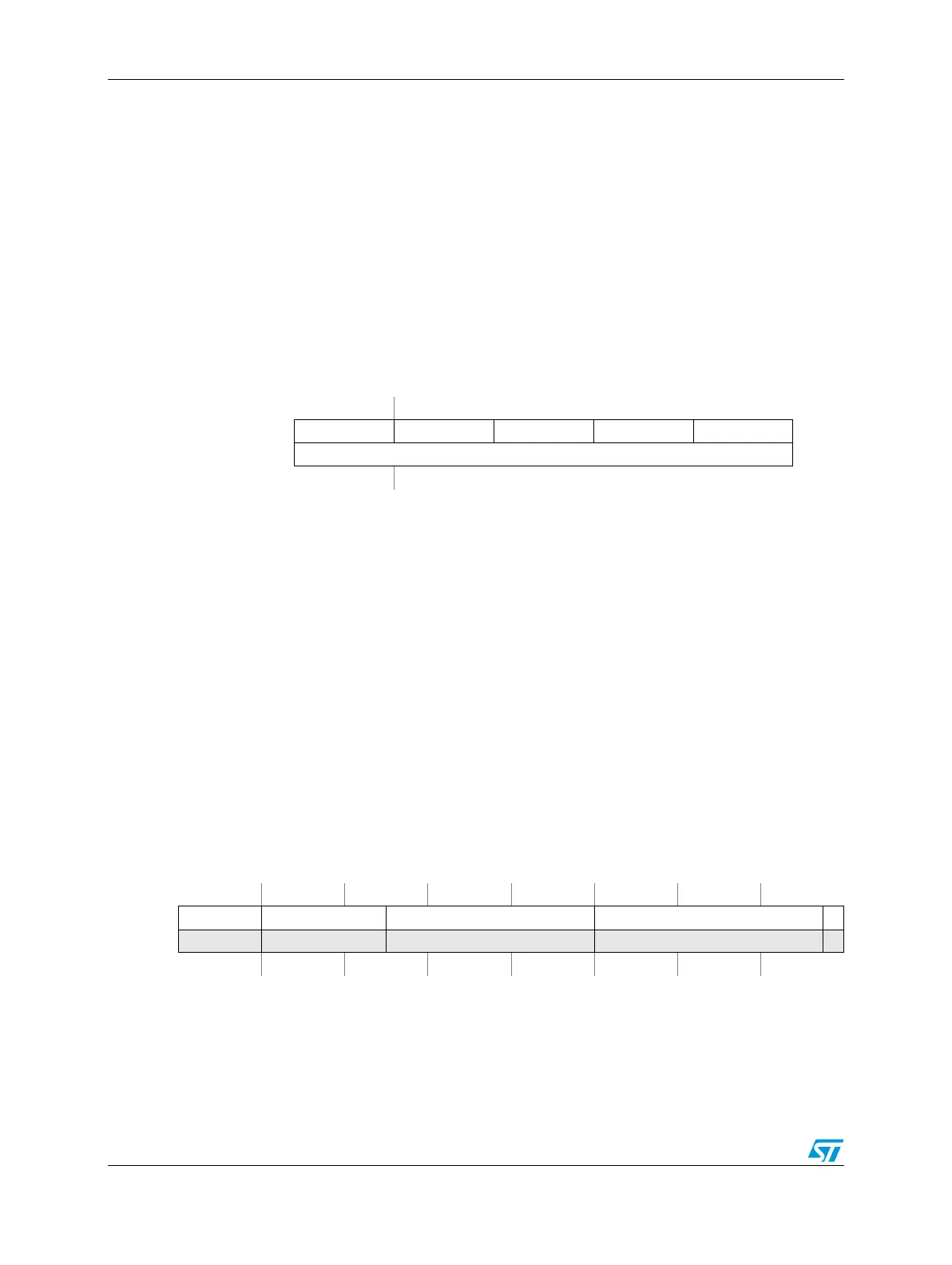
Figure 498. 5-bit Instruction register
43210
R1 0 1 01
W Instruction Code
Reset00001
Figure 499. Device identification register
IR[4:0]: 0_0001 (IDCODE) Access: User read-only
012345678910111213141516171819202122232425262728293031
R PRN DC PIN MIC ID
W
Reset00001010111000100010000001000001