RM0046 IEEE 1149.1 Test Access Port Controller (JTAGC)
Doc ID 16912 Rev 5 841/936
35 IEEE 1149.1 Test Access Port Controller (JTAGC)
35.1 Introduction
The JTAG port of the device consists of three inputs and one output. These pins include test
data input (TDI), test mode select (TMS), test clock input (TCK) and test data output (TDO).
TDI, TMS, TCK and TDO are compliant with the IEEE 1149.1-2001 standard and are shared
with the NDI through the test access port (TAP) interface.
35.2 Block diagram
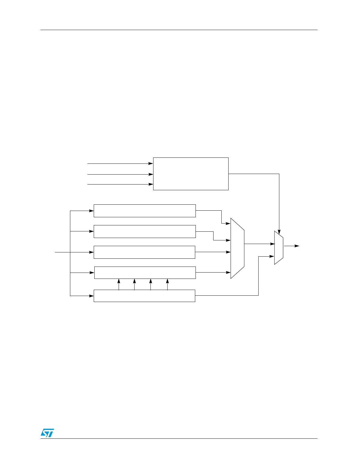
Figure 497 is a block diagram of the JTAG Controller (JTAGC).
Figure 497. JTAG controller block diagram
35.3 Overview
The JTAGC provides the means to test device functionality and connectivity while remaining
transparent to system logic when not in test mode. Testing is performed via a boundary scan
technique, as defined in the IEEE 1149.1-2001 standard. In addition, instructions can be
executed that allow the Test Access Port (TAP) to be shared with other modules on the
MCU. All data input to and output from the JTAGC is communicated in serial format.
TCK
TMS
TDI
Test access port (TAP)
TDO
32-bit device identification register
Boundary scan register
controller
1-bit bypass register
5-bit TAP instruction decoder
5-bit TAP instruction register
Power-on
reset