RM0046 System Integration Unit Lite (SIUL)
Doc ID 16912 Rev 5 259/936
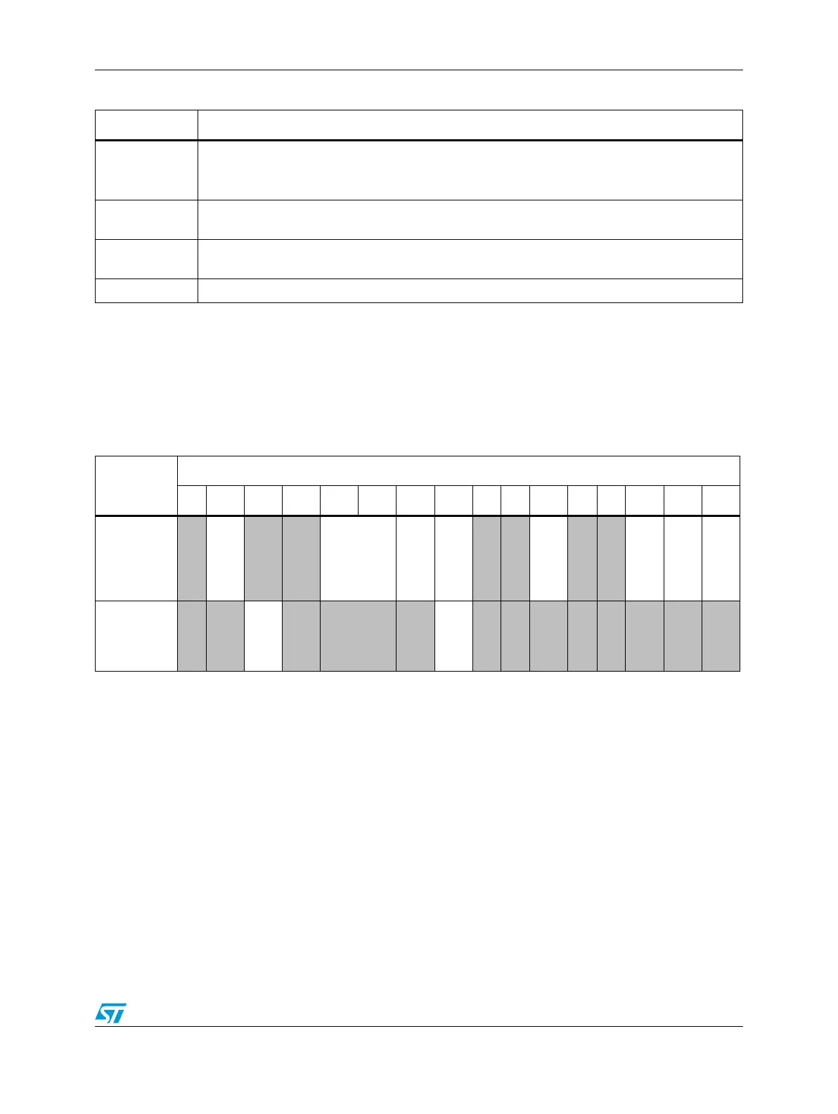
In addition to the bit map above, the following Table 100 [PCR bit implementation by pad
type] describes the PCR depending on the pad type (refer to Section 3.3.3: Pin multiplexing
for pad types description). The bits in shaded fields are not implemented for the particular
I/O type. The PA field selecting the number of alternate functions may or may not be present
depending on the number of alternate functions actually mapped on the pad.
Pad Selection for Multiplexed Inputs registers (PSMI[0_3:32_35])
The purpose of the PSMI[0_3:32_35] registers is to allow connecting a single input pad to
one of several peripheral inputs. Thus, it is possible to define different pads to be possible
inputs for a certain peripheral function.
Table 99. PCR[n] reset value exceptions
Field Description
PCR[2]
PCR[3]
PCR[4]
These registers correspond to the ABS[0], ABS[1], and FAB boot pins, respectively. Their default
state is input, pull enabled. Their reset value is 0x0102.
PCR[20]
This register corresponds to the TDO pin. Its default state is ALT1, slew rate = 1. Its reset value is
0x0604.
PCR[21]
This register corresponds to the TDI pin. Its default state is input, pull enabled, pull selected,
slew enabled. So its reset value is 0x0107.
PCR[n] For other PCR[n] registers, the reset value is 0x0000.
Table 100. PCR bit implementation by pad type
Pad type
PCR bit No.
0 1 2 3 4 5 6 7 8 9 10 11 12 13 14 15
S, M, F (Pad
with GPIO
and digital
alternate
functionality)
SMC APC PA [1:0] OBE IBE ODE SRC WPE WPS
I (Pad with
GPIO and
analog
functionality)
SMC APC PA [1:0] OBE IBE ODE SRC WPE WPS