Clock Generation Module (MC_CGM) RM0046
118/936 Doc ID 16912 Rev 5
5.2 Features
The MC_CGM includes the following features:
● generates system and peripheral clocks
● selects and enables/disables the system clock supply from system clock sources
according to MC_ME control
● contains a set of registers to control clock dividers for divided clock generation
● contains a set of registers to control peripheral clock selection
● supports multiple clock sources and maps their address spaces to its memory map
● generates an output clock
● guarantees glitch-less clock transitions when changing the system clock selection
● supports 8, 16 and 32-bit wide read/write accesses
5.3 External Signal Description
The MC_CGM delivers an output clock to the PAD[22] pin for off-chip use and/or
observation.
5.4 Memory Map and Register Definition
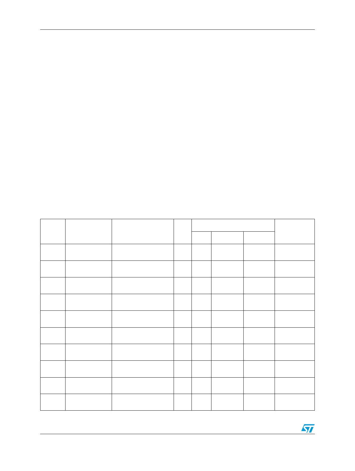
Table 24. MC_CGM Register Description
Address Name Description Size
Access
Location
User Supervisor Test
0xC3FE
_0370
CGM_OC_EN Output Clock Enable word read read/write read/write on page 5-124
0xC3FE
_0374
CGM_OCDS_SC
Output Clock Division
Select
byte read read/write read/write on page 5-124
0xC3FE
_0378
CGM_SC_SS
System Clock Select
Status
byte read read read on page 5-125
0xC3FE
_037C
CGM_SC_DC0
System Clock Divider
Configuration 0
byte read read/write read/write on page 5-126
0xC3FE
_0380
CGM_AC0_SC
Aux Clock 0 Select
Control
word read read/write read/write on page 5-127
0xC3FE
_0384
CGM_AC0_DC0
Aux Clock 0 Divider
Configuration 0
byte read read/write read/write on page 5-128
0xC3FE
_0388
CGM_AC1_SC
Aux Clock 1 Select
Control
word read read/write read/write on page 5-128
0xC3FE
_038C
CGM_AC1_DC0
Aux Clock 1 Divider
Configuration 0
byte read read/write read/write on page 5-129
0xC3FE
_0390
CGM_AC2_SC
Aux Clock 2 Select
Control
word read read/write read/write on page 5-130
0xC3FE
_0394
CGM_AC2_DC0
Aux Clock 2 Divider
Configuration 0
byte read read/write read/write on page 5-131