Flash Memory RM0046
332/936 Doc ID 16912 Rev 5
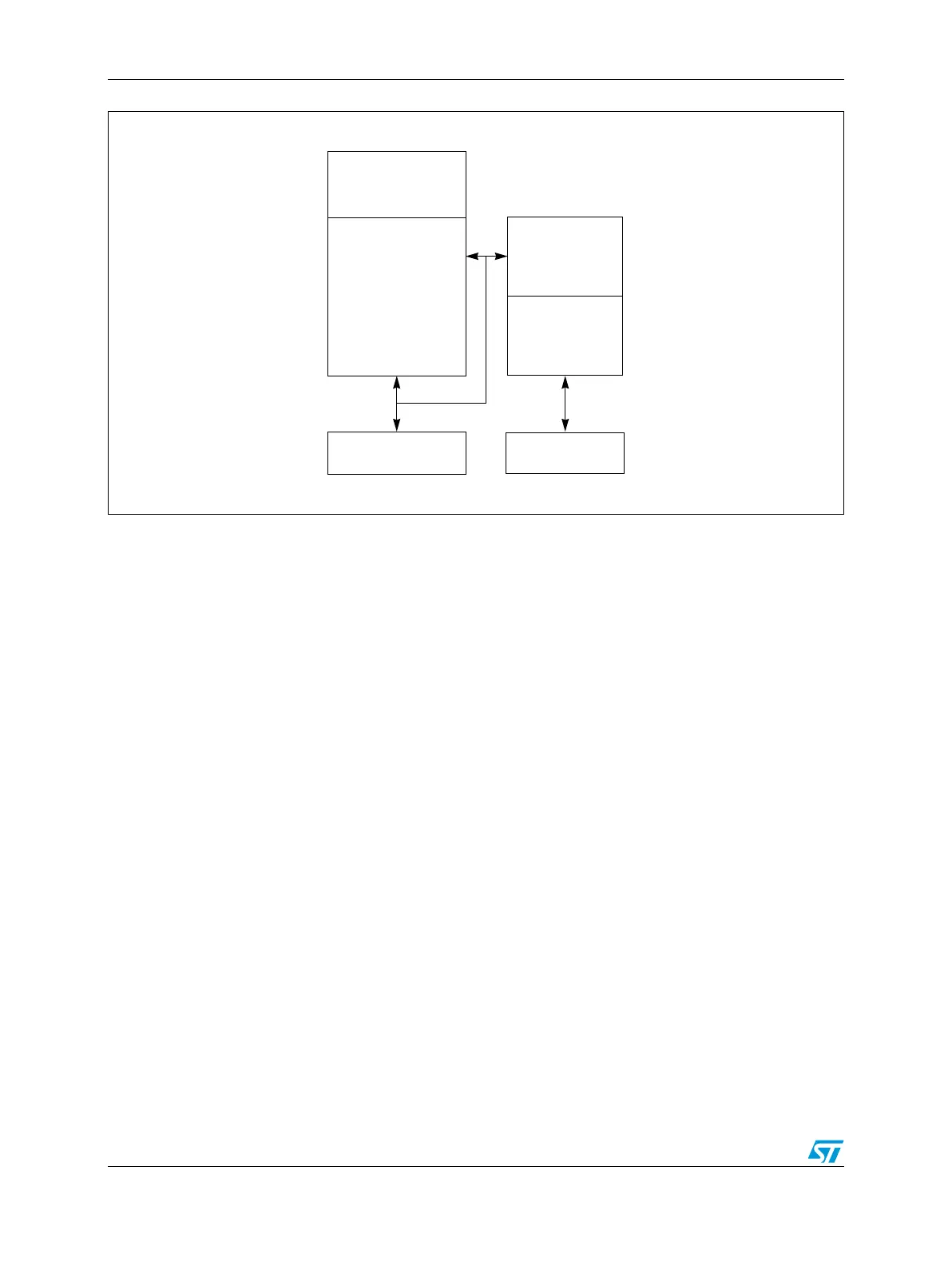
Figure 152. Code Flash module structure
17.3.4 Functional description
Macrocell structure
The Flash macrocell provides high density non-volatile memories with high-speed read
access.
The Flash module is addressable by word (32 bits) or double-word (64 bits) for
programming, and by page (128 bits) for reads. Reads done to the Flash always return 128
bits, although read page buffering may be done in the platform BIU.
Each read of the Flash module retrieves a page, or 4 consecutive words (128 bits) of
information. The address for each word retrieved within a page differ from the other
addresses in the page only by address bits (3:2).
The Flash page read architecture supports both cache and burst mode at the BIU level for
high-speed read application.
The Flash module supports fault tolerance through Error Correction Code (ECC) and/or
error detection. The ECC implemented within the Flash module will correct single bit failures
and detect double bit failures.
The Flash module uses an embedded hardware algorithm implemented in the memory
interface to program and erase the Flash core.
Control logic that works with the software block enables, and software lock mechanisms, is
included in the embedded hardware algorithm to guard against accidental program/erase.
The hardware algorithm perform the steps necessary to ensure that the storage elements
are programmed and erased with sufficient margin to guarantee data integrity and reliability.
A programmed bit in the Flash module reads as logic level 0 (or low).
+ 16 KB TestFlash
HV generator
Matrix
Registers
Interface
Flash Bank 0
Interface
+ 16 KB Shadow
Flash
Controller
Code Flash
Program/Erase
Registers
256 KB