FlexPWM RM0046
690/936 Doc ID 16912 Rev 5
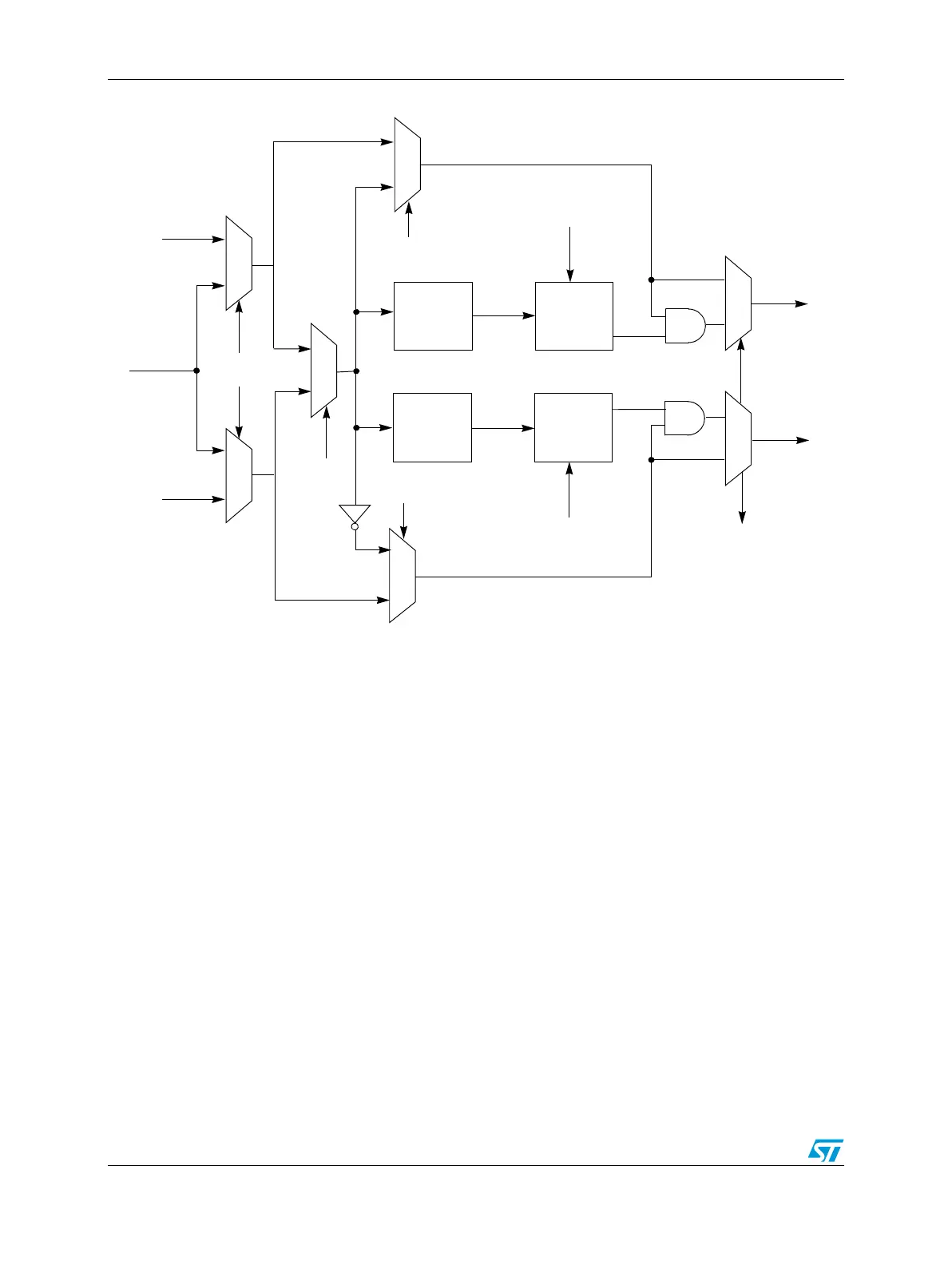
Figure 376. Deadtime insertion and fine control logic
While in the complementary mode, a PWM pair can be used to drive top/bottom transistors,
as shown in Figure 376. When the top PWM channel is active, the bottom PWM channel is
inactive, and vice versa.
Note: To avoid short-circuiting the DC bus and endangering the transistor, there must be no
overlap of conducting intervals between top and bottom transistor. However, the transistor’s
characteristics may cause its switching-off time to be longer than its switching-on time. To
avoid the conducting overlap of top and bottom transistors, deadtime needs to be inserted in
the switching period, as illustrated in Figure 377.
The deadtime generators automatically insert software-selectable activation delays into the
pair of PWM outputs. The deadtime registers (DTCNT0 and DTCNT1) specify the number of
IPBus clock cycles to use for deadtime delay. Every time the deadtime generator inputs
change state, deadtime is inserted. Deadtime forces both PWM outputs in the pair to the
inactive state.
When deadtime is inserted in complementary PWM signals connected to an inverter driving
an inductive load, the PWM waveform on the inverter output will have a different duty cycle
than what appears on the output pins of the PWM module. This results in a distortion in the
voltage applied to the load. A method of correcting this, adding to or subtracting from the
PWM value used, is discussed next.
PWMA
from Force
Out logic
PWMA
rising
edge
detect
down
counter
start
DTCNT0
zero
PWMB
detect
edge
falling
counter
down
start
DTCNT1
zero
to Output
logic
0
1
IPOL
1
0
INDEP
0
1
0
1
INDEP
0
1
INDEP
0
1
DBLEN
PWMB
0
1
DBLPWM