RM0046 IEEE 1149.1 Test Access Port Controller (JTAGC)
Doc ID 16912 Rev 5 845/936
35.7.4 Boundary scan register
The boundary scan register is connected between TDI and TDO when the EXTEST,
SAMPLE or SAMPLE/PRELOAD instructions are active. It captures input pin data, forces
fixed values on output pins, and selects a logic value and direction for bidirectional pins.
Each bit of the boundary scan register represents a separate boundary scan register cell, as
described in the IEEE 1149.1-2001 standard and discussed in Section 35.8.5, “Boundary
scan. The size of the boundary scan register is 464 bits.
35.8 Functional description
35.8.1 JTAGC reset configuration
While in reset, the TAP controller is forced into the test-logic-reset state, thus disabling the
test logic and allowing normal operation of the on-chip system logic. In addition, the
instruction register is loaded with the IDCODE instruction.
35.8.2 IEEE 1149.1-2001 (JTAG) Test Access Port (TAP)
The JTAGC uses the IEEE 1149.1-2001 Test Access Port (TAP) for accessing registers.
This port can be shared with other TAP controllers on the MCU. For more detail on TAP
sharing via JTAGC instructions refer to Section , “ACCESS_AUX_TAP_x instructions.
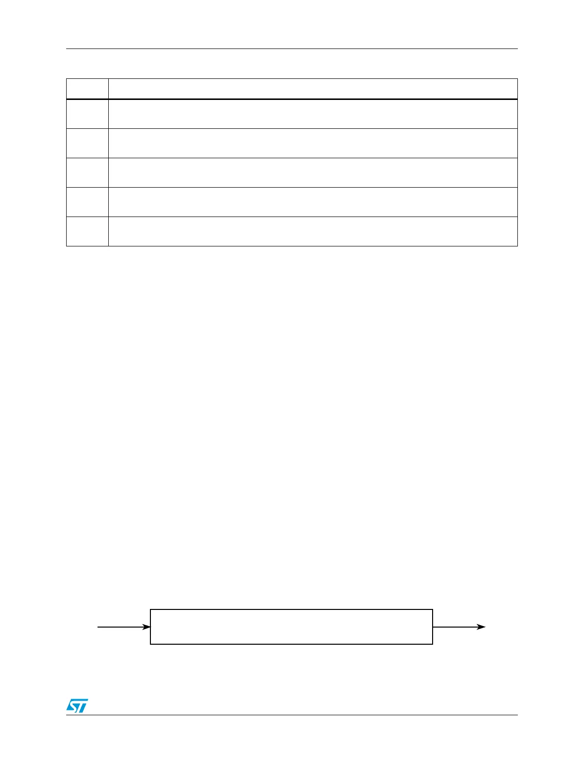
Data is shifted between TDI and TDO though the selected register starting with the least
significant bit, as illustrated in Figure 500. This applies for the instruction register, test data
registers, and the bypass register.
Figure 500. Shifting data through a register
Table 455. Device identification register field descriptions
Field Description
0–3
PRN
Part revision number. Contains the revision number of the device. This field changes with each revision
of the device or module.
4–9
DC
Design center. For the SPC560P40/34 this value is 0x2B.
10–19
PIN
Part identification number. Contains the part number of the device. For the SPC560P40/34, this value is
0x222.
20–30
MIC
Manufacturer identity code. Contains the reduced Joint Electron Device Engineering Council (JEDEC)
ID for STMicroelectronics, 0x20.
31
ID
IDCODE register ID. Identifies this register as the device identification register and not the bypass
register. Always set to 1.
Selected register
MSB
LSB
TDI
TDO

 Loading...