RM0046 Deserial Serial Peripheral Interface (DSPI)
Doc ID 16912 Rev 5 473/936
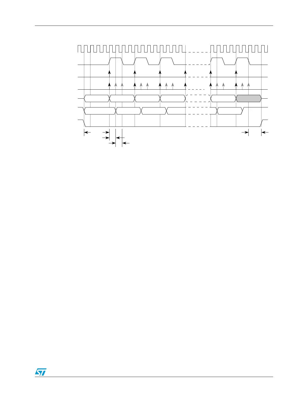
Figure 222. DSPI modified transfer format (MTFE = 1, CPHA = 0, f
SCK
= f
SYS
/ 4)
Modified SPI transfer format (MTFE = 1, CPHA = 1)
At the start of a transfer the DSPI asserts the CS signal to the slave device. After the CS to
SCK delay has elapsed the master and the slave put data on their SOUT pins at the first
edge of SCK. The slave samples the master SOUT signal on the even numbered edges of
SCK. The master samples the slave SOUT signal on the odd numbered SCK edges starting
with the 3rd SCK edge. The slave samples the last bit on the last edge of the SCK. The
master samples the last slave SOUT bit one half SCK cycle after the last edge of SCK. No
clock edge is visible on the master SCK pin during the sampling of the last bit. The SCK to
CS delay must be programmed to be greater than or equal to half the SCK period.
Note: For the modified transfer format to operate correctly, you must thoroughly analyze the SPI
link timing budget.
Figure 223 shows the modified transfer format for CPHA = 1. Only the condition where
CPOL = 0 is shown.
t
CSC
= CS to SCK delay.
t
ASC
= After SCK delay.
System clock
123456
CSx
t
ASC
SCK
Master sample
Slave SOUT
Master SOUT
System clock
System clock
Slave sample
t
CSC