System Integration Unit Lite (SIUL) RM0046
264/936 Doc ID 16912 Rev 5
Masked Parallel GPIO Pad Data Out register 0–6 (MPGPDO[0:6])
This register can be used to selectively modify the pad values associated to PPDO[x][15:0].
The MPGPDO[x] register may only be accessed with 32-bit writes. 8-bit or 16-bit writes will
not modify any bits in the register and cause a transfer error response by the module. Read
accesses will return 0.
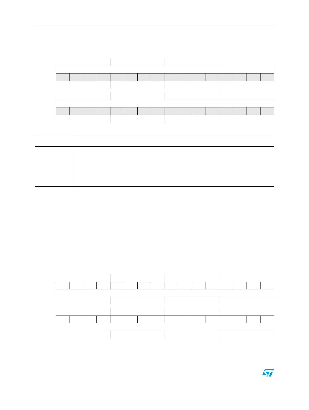
Figure 110. Parallel GPIO Pad Data In register 0–3 (PGPDI[0:3])
Address:
Base + 0x0C40 (PGPDI0)
Base + 0x0C44 (PGPDI1)
Base + 0x0C45 (PGPDI2)
Base + 0x0C4C (PGPDI3)
Access: User read-only
0123456789101112131415
R PPDI[x][15:0]
W
Reset0000000000000000
16 17 18 19 20 21 22 23 24 25 26 27 28 29 30 31
R PPDI[x + 1][15:0]
W
Reset0000000000000000
Table 106. PGPDI[0:3] field descriptions
Field Description
PPDI[x]
Parallel Pad Data In
Read the current pad value. Accesses to this register location are coherent with accesses to the
bit-wise GPIO Pad Data Input registers 0_3–68_71 (GPDI[0_3:68_71]).
The x and bit index define which PPDI register bit is equivalent to which PDI register bit
according to the following equation:
PPDI[x][y]=PDI[(x *16)+y]
Figure 111. Masked Parallel GPIO Pad Data Out register 0–6 (MPGPDO[0:6])
Address:
Base + 0x0C80 (MPGPDO0)
Base + 0x0C84 (MPGPDO1)
Base + 0x0C88 (MPGPDO2)
Base + 0x0C8C (MPGPDO3)
Base + 0x0C80 (MPGPDO4)
Base + 0x0C84 (MPGPDO5)
Base + 0x0C98 (MPGPDO6)
Access: User write-only
0123456789101112131415
R000000 0000000 000
W MASK[x][15:0]
Reset0000000000000000
16 17 18 19 20 21 22 23 24 25 26 27 28 29 30 31
R 0 000000000000000
W MPPDO[x][15:0]
Reset0000000000000000