RM0046 Clock Generation Module (MC_CGM)
Doc ID 16912 Rev 5 123/936
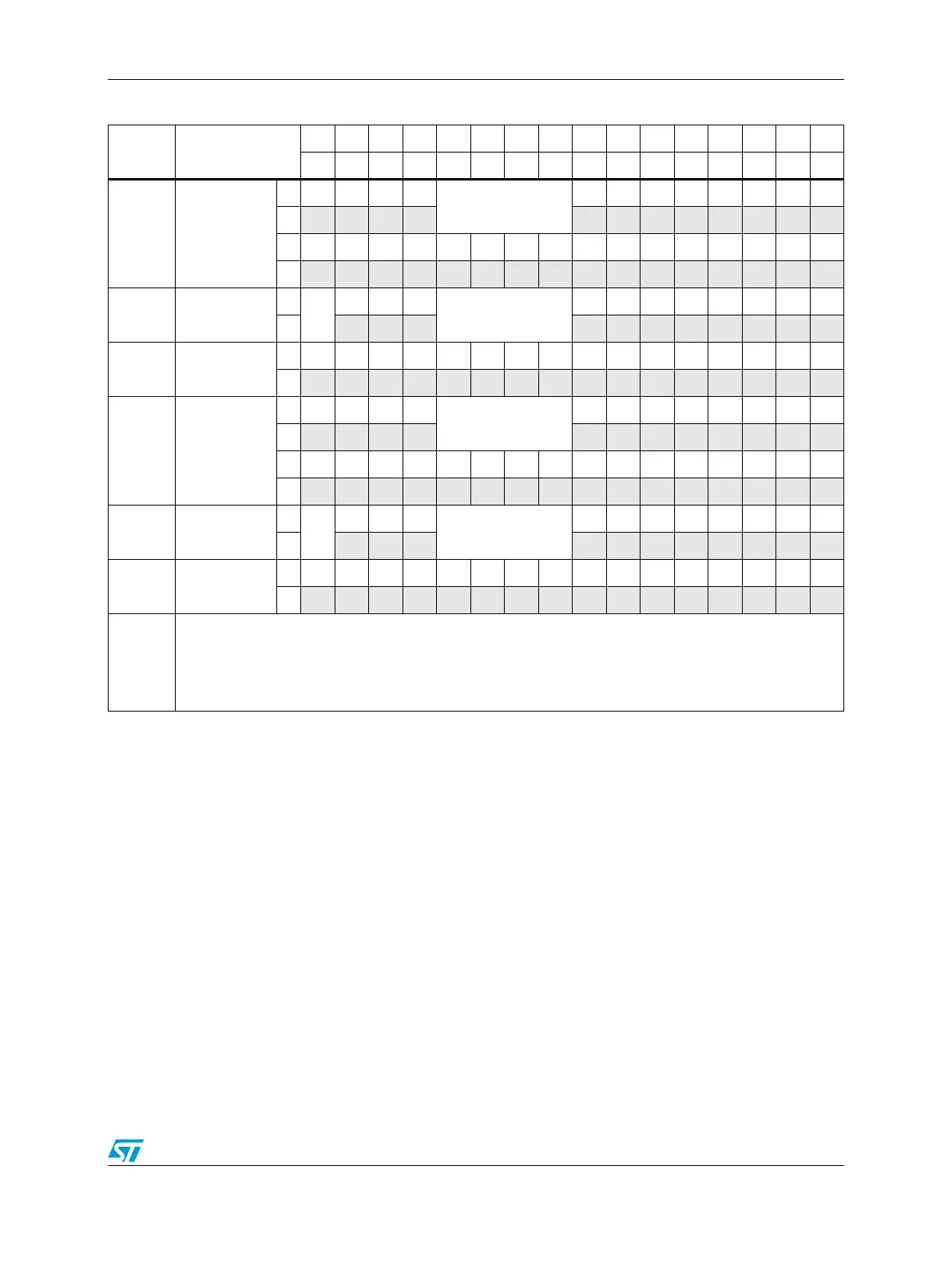
5.5 Register Descriptions
All registers may be accessed as 32-bit words, 16-bit half-words, or 8-bit bytes. The bytes
are ordered according to big endian. For example, the CGM_OC_EN register may be
accessed as a word at address 0xC3FE_0370, as a half-word at address 0xC3FE_0372, or
as a byte at address 0xC3FE_0373.
0xC3FE
_0388
CGM_AC1_S
C
R0000
SELCTL
00000000
W
R0000000000000000
W
0xC3FE
_038C
CGM_AC1_D
C0
R
DE0
000
DIV0
00000000
W
R0000000000000000
W
0xC3FE
_0390
CGM_AC2_S
C
R0000
SELCTL
00000000
W
R0000000000000000
W
0xC3FE
_0394
CGM_AC2_D
C0
R
DE0
000
DIV0
00000000
W
R0000000000000000
W
0xC3FE
_0398
…
0xC3FE
_3FFC
reserved
Table 25. MC_CGM Memory Map (continued)
Address Name
0123456789101112131415
16 17 18 19 20 21 22 23 24 25 26 27 28 29 30 31