System Integration Unit Lite (SIUL) RM0046
260/936 Doc ID 16912 Rev 5
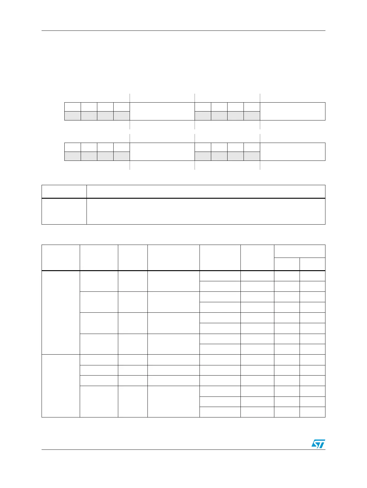
Figure 106. Pad Selection for Multiplexed Inputs registers (PSMI[0_3:32_35])
Address:
Base + 0x0500 (PSMI0_3)
Base + 0x0504 (PSMI4_7)
Base + 0x0508 (PSMI8_11)
Base + 0x050C (PSMI12_15)
Base + 0x0510 (PSMI16_19)
Base + 0x0514 (PSMI20_23)
Base + 0x0518 (PSMI024_27)
Base + 0x051C (PSMI28_31)
Base + 0x0520 (PSMI32_35)
Access: User read/write
0123456789101112131415
R0000
PADSEL0[3:0]
0000
PADSEL1[3:0]
W
Reset0000000000000000
16 17 18 19 20 21 22 23 24 25 26 27 28 29 30 31
R0000
PADSEL2[3:0]
0 000
PADSEL3[3:0]
W
Reset0000000000000000
Table 101. PSMI[0_3:32_35] field descriptions
Field Description
PADSEL0–3
...
PADSEL32–35
Pad Selection Bits
Each PADSEL field selects the pad currently used for a certain input function. See Table 102 Pad
selection.
Table 102. Pad selection
Register PADSEL Module Port
PADSEL[3:0]
value
(1)
Port name
LQFP pin
64-pin 100-pin
PSMI0_3
(2)
PADSEL0 ctu0 EXT_IN
0000 C[13] — 71
0001 C[15] — 85
PADSEL1 dspi2 SCK
0000 A[0] — 51
0001 A[11] 53 82
PADSEL2 dspi2 SIN
0000 A[2] — 57
0001 A[13] 61 95
PADSEL3 dspi2 CS0
0000 A[3] 41 64
0001 A[10] 52 81
PSMI4_7
(3)
PADSEL0 — — — — — —
PADSEL1 — — — — — —
PADSEL2 — — — — — —
PADSEL3 eTimer0 ETC[4]
0000 A[4] 48 75
0001 C[11] 33 55
0010 B[14] — 44