RM0046 Analog-to-Digital Converter (ADC)
Doc ID 16912 Rev 5 581/936
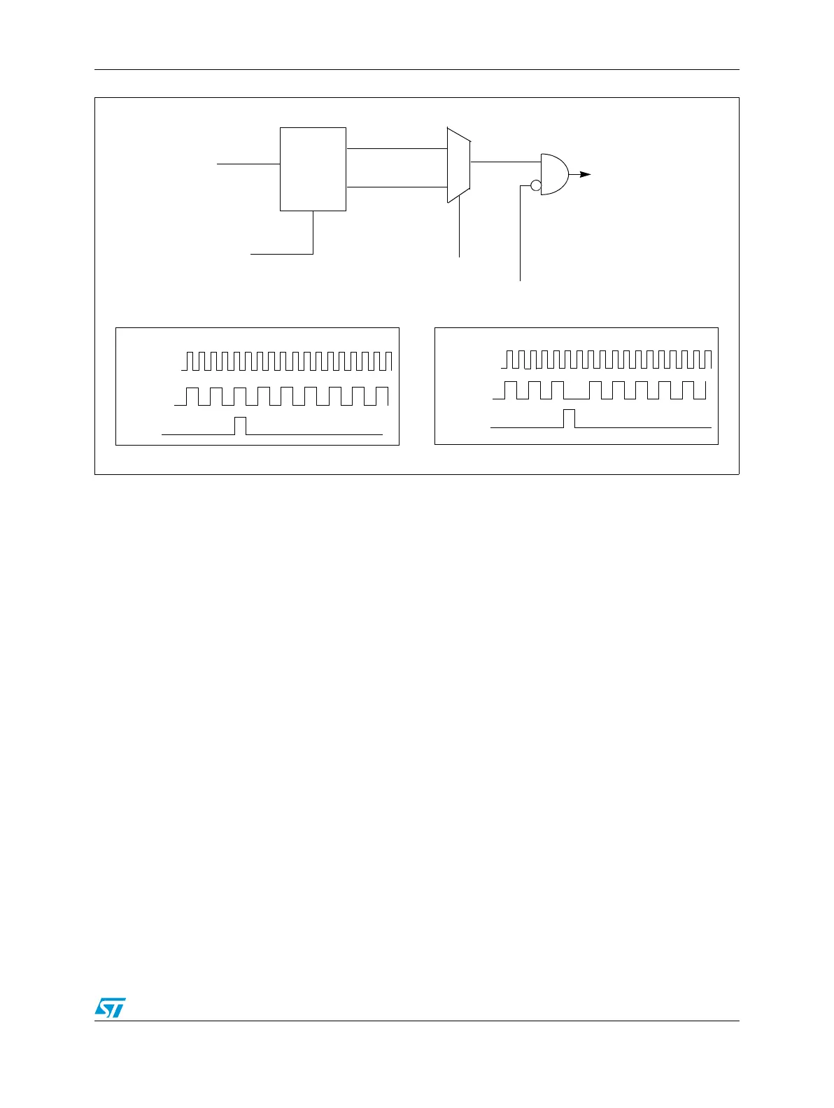
Figure 282. Prescaler simplified block diagram
The clock stretching is implemented if and only if ADCLKSEL = 0 (and clock is half of the
MC_PLL_CLK).
23.3.3 ADC sampling and conversion timing
In order to support different loading and switching times, several different Conversion Timing
registers (CTR) are present. There is one register per channel type. INPLATCH and
INPCMP configurations are limited when the system clock frequency is greater than
20 MHz.
When a conversion is started, the ADC connects the internal sampling capacitor to the
respective analog input pin, allowing the capacitance to charge up to the input voltage value.
The time to load the capacitor is referred to as sampling time. After completion of the
sampling phase, the evaluation phase starts and all the bits corresponding to the resolution
of the ADC are estimated to provide the conversion result.
The conversion times are programmed via the bit fields of the CTR. Bit fields INPLATCH,
INPCMP, and INPSAMP define the total conversion duration (T
conv
) and in particular the
partition between sampling phase duration (T
sample
) and total evaluation phase duration
(T
eval
).
ADC_0
Figure 283 represents the sampling and conversion sequence.
CTU trigger signal
ADCClk
MC_PLL_CLK
Clock
Prescaler
CTU trigger signal
MC_PLL_CLK
ADCClk
MC_PLL_CLK
ADCClk
CTU trigger signal
ADCLKSEL
MC_PLL_CLK
MC_PLL_CLK/2
ADCLKSEL = ‘0’
ADCLKSEL = ‘0’ (clock stretched)
ACKO