RM0046 Functional Safety
Doc ID 16912 Rev 5 739/936
Area 3 is 6 KB, starting at address 0x2000 and is a mirror of area 1. A read/write access to
these 0x2000 + X addresses will read/write the register at address X. As a side effect, a
write access to address 0x2000 + X will set the optional Soft Lock Bits for this address X in
the same cycle as the register at address X is written. Not all registers in area 1 need to
have protection defined by associated Soft Lock Bits. For unprotected registers at address
Y, accesses to address 0x2000 + Y will be identical to accesses at address Y. Only for
registers implemented in area 1 and defined as protectable Soft Lock Bits will be available in
area 4.
Area 4 is 1.5 KB and holds the Soft Lock Bits, one bit per byte in area 1. The four Soft Lock
Bits associated with one module register word are arranged at byte boundaries in the
memory map. The Soft Lock Bit registers can be directly written using a bit mask.
Area 5 is 512 bytes and holds the configuration bits of the protection mode. There is one
configuration hard lock bit per module that prevents all further modifications to the Soft Lock
Bits and can only be cleared by a system reset once set. The other bits, if set, will allow user
access to the protected module.
If any locked byte is accessed with a write transaction, a transfer error will be issued to the
system and the write transaction will not be executed. This is true even if not all accessed
bytes are locked.
Accessing unimplemented 32-bit registers in areas 4 and 5 will result in a transfer error.
Register protection memory map
Table 387 shows the registers in the Safety Port.
Note: Reserved registers in area #2 will be handled according to the protected IP (module under
protection).
Registers description
This section describes in address order all the register protection registers. Each description
includes a standard register diagram with an associated figure number. Details of register bit
and field function follow the register diagrams, in bit order.
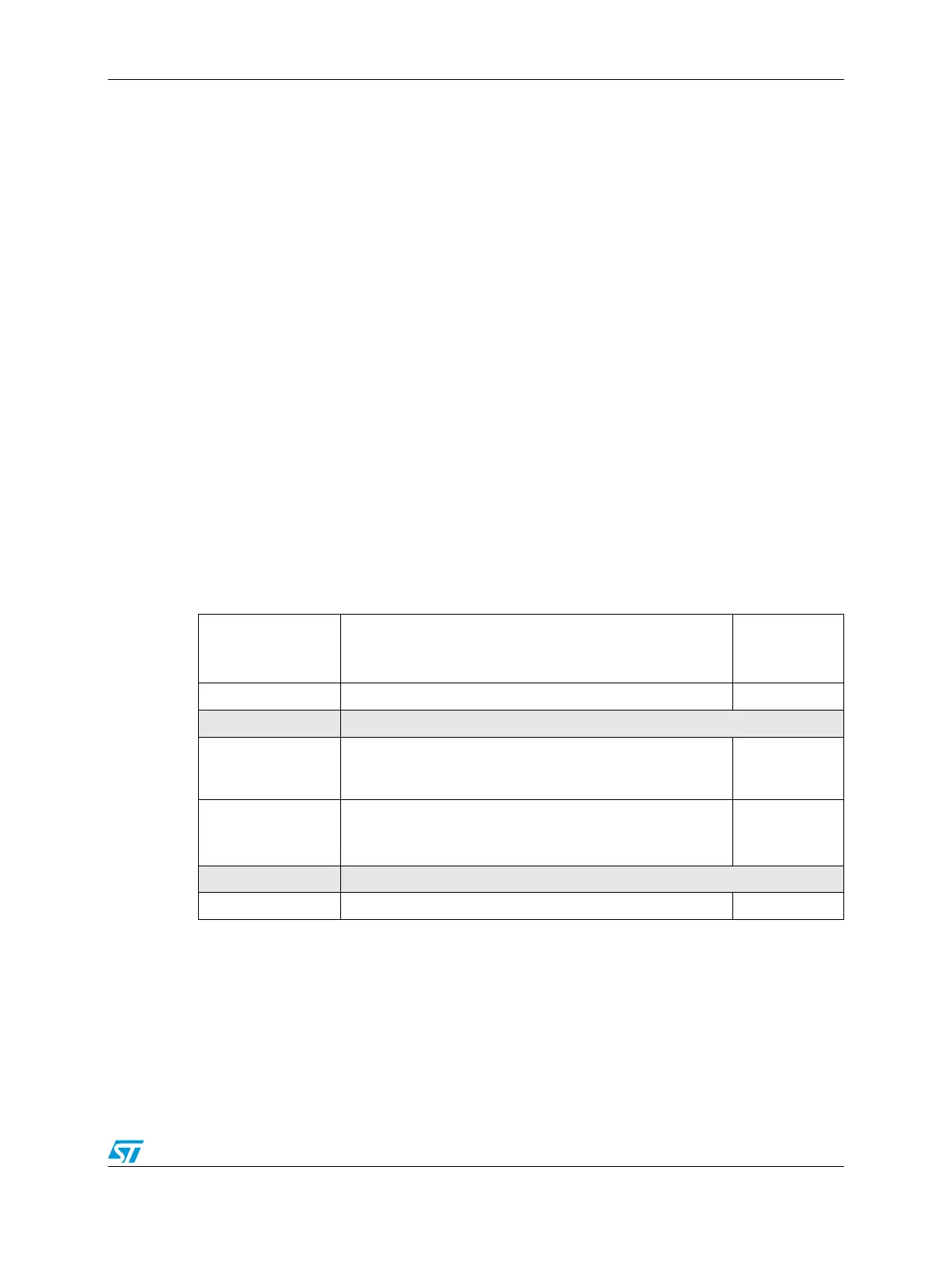
Table 387. Register protection memory map
Offset from
REG_ PROT_BASE
(0xFFFE_8000)
Register Location
0x0000–0x17FF Module Register 0 (MR0)–Module Register 6143(MR6143) on page 27-740
0x1800–0x1FFF Reserved
0x2000–0x37FF
Module Register 0 (MR0) + Set Soft Lock Bit 0 (LMR0)–
Module Register 6143 (MR6143) + Set Soft Lock Bit 6143
(LMR6143)
on page 27-740
0x3800–0x3DFF
Soft Lock Bit Register 0 (SLBR0): Soft Lock Bits 0:3–
Soft Lock Bit Register 1535 (SLBR1535): Soft Lock Bits
6140:6143
on page 27-740
0x3E00–0x3FFB Reserved
0x3FFC Global Configuration Register (GCR) on page 27-741