Functional Safety RM0046
744/936 Doc ID 16912 Rev 5
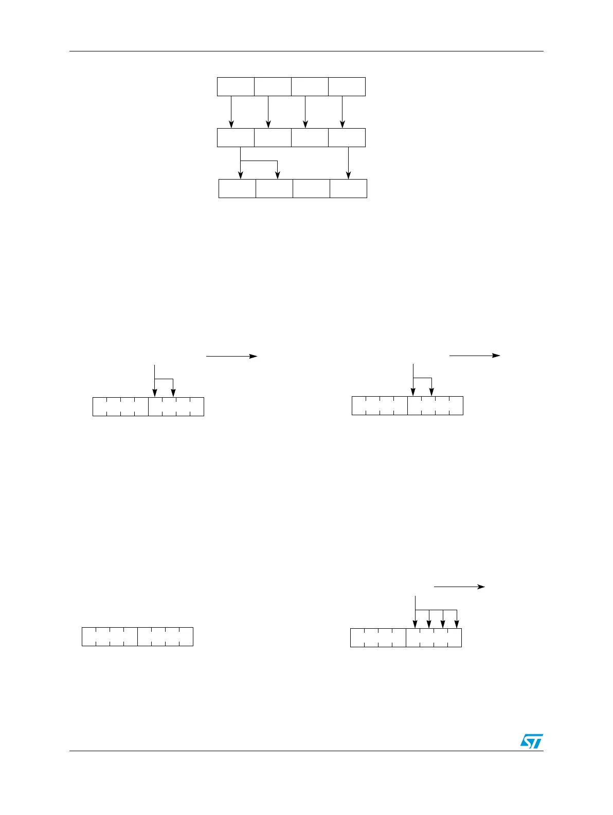
Figure 425. Change lock settings for mixed protection
The data written to SLBRn[SLB0] is mirrored to SLBRn[SLB1] as the corresponding register
is 16-bit protected. The data written to SLBRn[SLB2] is blocked as the corresponding
register is unprotected. The data written to SLBRn[SLB3] is written to SLBRn[SLB3].
Enable locking via mirror module space (area #3)
It is possible to enable locking for a register after writing to it. To do so the mirrored module
address space must be used. Figure 426 shows one example.
Figure 426. Enable locking via mirror module space (area #3)
When writing to address 0x0008 the registers MR9 and MR8 in the protected module are
updated. The corresponding lock bits remain unchanged (left part of Figure 423).
When writing to address 0x2008 the registers MR9 and MR8 in the protected module are
updated. The corresponding lock bits SLBR2.SLB[1:0] are set while the lock bits
SLBR2.SLB[3:2] remain unchanged (right part of Figure 423).
Figure 427 shows an example where some addresses are protected and some are not.
Figure 427. Enable locking for protected and unprotected addresses
SLB0 SLB1 0 SLB3
SLBR
update lock bits
1SLBRn[WE[3:0]]
to SLB0
write data
to SLB1 to SLB2 to SLB3
XX1
SLBR2
WE[3:0]
00000000
SLB[3:0]
16-bit write to address 0x0008
no change
write to
MR[9:8]
SLBR2
WE[3:0]
00001100
SLB[3:0]
16-bit write to address 0x2008
set lock bits
write to
MR[9:8]
SLBR3
WE[3:0]
00000000
SLB[3:0]
Before write access
SLBR3
WE[3:0]
00000011
SLB[3:0]
32-bit write to address 0x200C
set lock bits
write to
MR[15:12]
After
write access