RM0046 Clock Description
Doc ID 16912 Rev 5 101/936
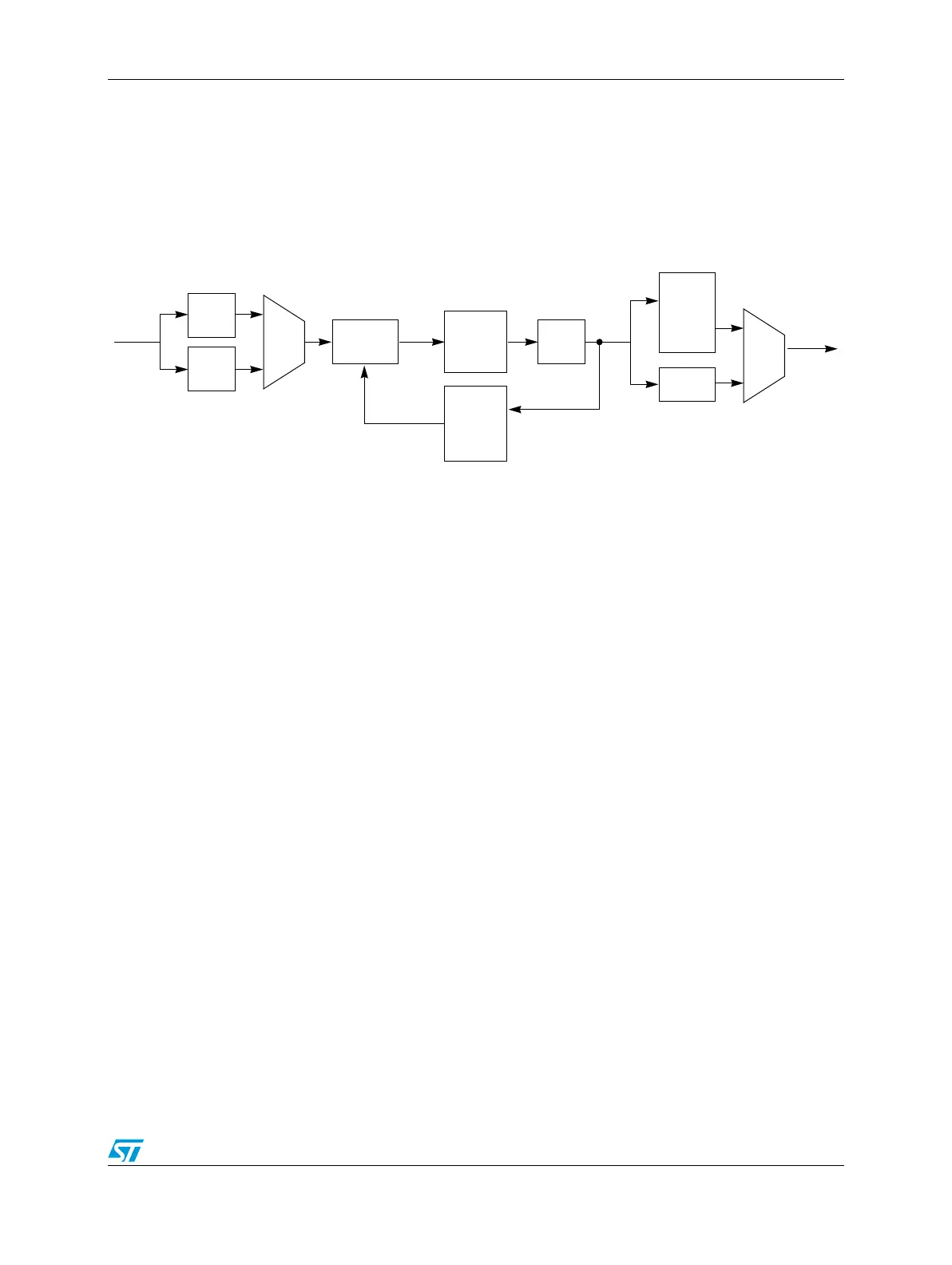
4.8.2 Overview
The FMPLL enables the generation of high speed system clocks from a common 4–40 MHz
input clock. Further, the FMPLL supports programmable frequency modulation of the
system clock. The PLL multiplication factor and output clock divider ratio are all software
configurable.
The FMPLL block diagram is shown in Figure 14.
Figure 14. FMPLL block diagram
4.8.3 Features
The FMPLL has the following major features:
● Input clock frequency 4–40 MHz
● Voltage controlled oscillator (VCO) range from 256 MHz to 512 MHz
● Reduced frequency divider (RFD) for reduced frequency operation without forcing the
FMPLL to relock
● Frequency modulated PLL
– Modulation enabled/disabled through software
– Triangle wave modulation
● Programmable modulation depth
– ±0.25% to ±4% deviation from center spread frequency
– –0.5% to +8% deviation from down spread frequency
– Programmable modulation frequency dependent on reference frequency
● Self-clocked mode (SCM) operation
● 4 available modes
– Normal mode
– Progressive clock switching
– Normal Mode with SSCG
– Powerdown mode
4.8.4 Memory map
Table 1 2 shows the memory map locations. Addresses are given as offsets of the module
base address.
BUFFER
Charge
Pump
Low Pass
Filter
VCO
IDF
DIV2
Loop
Division
Factor
XOSC
Output
PHI
(LDF)
CR[NDIV]
Division
Factor
(ODF)
CR[ODF]
DIV4