Flash Memory RM0046
360/936 Doc ID 16912 Rev 5
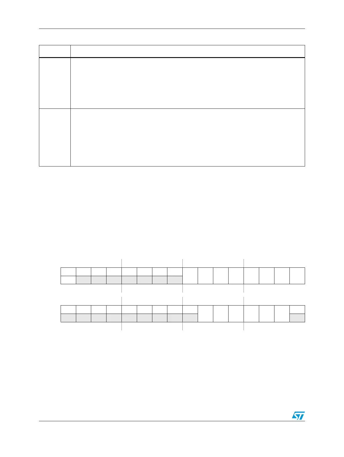
User Test 0 register (UT0)
The User Test feature gives the user of the Flash module the ability to perform test features
on the Flash. The User Test 0 register allows controlling the way in which the Flash content
check is done.
The UT0[MRE], UT0[MRV], UT0[AIS], UT0[EIE], and DSI[7:0] bits are not accessible
whenever MCR[DONE] or UT0[AID] are low. Reads return indeterminate data. Writes have
no effect.
8-15
MxPFD
Master x Prefetch Disable (x = 0,1,2,...,7)
These bits control whether prefetching may be triggered based on the master number of the
requesting AHB master. This field is further qualified by the PFCR0[B0_Px_DPFE, B0_Px_IPFE,
Bx_Py_BFE] bits.
0 Prefetching may be triggered by this master.
1 No prefetching may be triggered by this master.
16-31
MxAP
Master x Access Protection (x = 0,1,2,...,7)
These fields control whether read and write accesses to the Flash are allowed based on the master
number of the initiating module.
00 No accesses may be performed by this master.
01 Only read accesses may be performed by this master.
10 Only write accesses may be performed by this master.
11 Both read and write accesses may be performed by this master.
Table 158. PFAPR field descriptions (continued)
Field Description
Figure 163. User Test 0 register (UT0)
Address:
Base + 0x003C Access: User read/write
0123456789101112131415
RUTE0000000
DSI7 DSI6 DSI5 DSI4 DSI3 DSI2 DSI1 DSI0
W w1c
Reset0000000000000000
16 17 18 19 20 21 22 23 24 25 26 27 28 29 30 31
R00000000 0
XMREMRVEIE AIS AIE
AID
W
Reset0000000000000001