RM0046 Voltage Regulators and Power Supplies
Doc ID 16912 Rev 5 839/936
Voltage Regulator Status register (VREG_STATUS)
34.2 Power supply strategy
The SPC560P40/34 provides three dedicated supply domains at the package level:
● HV—High voltage external power supply for I/Os, voltage regulator module, and most
analog modules
This must be provided externally through V
DD_HV
/V
SS_HV
power pins. Voltage values
should be aligned with V
DD
/V
SS
. Refer to the device datasheet for details.
● ADC—High voltage external power supply for ADC module
This must be provided externally through V
DD_HV_ADx
/V
SS_HV_ADx
power pins. Voltage
values should be aligned with V
DD_HV_ADx
/V
SS_HV_ADx
. Refer to the device datasheet
for details.
● LV—Low voltage internal power supply for core, PLL, and flash digital logic
This is provided to the core, PLL and flash. Five V
DD_LV
/V
SS_LV
pins pairs are provided
to connect the low voltage power supply. Refer to the device datasheet for details.
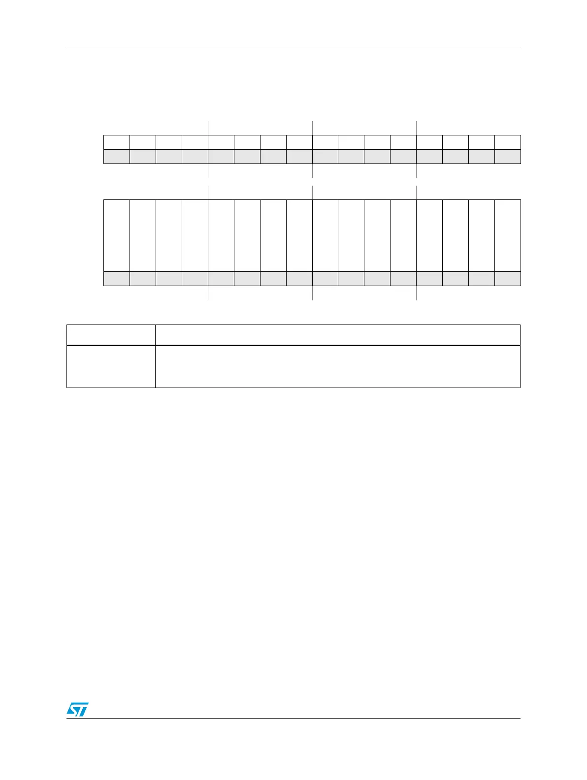
Figure 496. Voltage Regulator Status register (VREG_STATUS)
Address:
Base + 0x0084 Access: User read-only
0123456789101112131415
R00000000 00000 000
W
Reset0000000000000000
16 17 18 19 20 21 22 23 24 25 26 27 28 29 30 31
R000000010000000
5V_LVD_STATUS
W
Reset0000000100000001
Table 453. VREG_STATUS field descriptions
Field Description
5V_LVD_STATUS
Status bit for 5 V LVD from regulator
05 V LVD not OK
15 V LVD OK