RM0046 System Integration Unit Lite (SIUL)
Doc ID 16912 Rev 5 265/936
Interrupt Filter Maximum Counter registers 0–24 (IFMC[0:24])
These registers configure the filter counter associated with each digital glitch filter.
Table 107. MPGPDO[0:6] field descriptions
Field Description
MASK[x]
[15:0]
Mask Field
Each bit corresponds to one data bit in the MPPDO[x] field at the same bit location.
0: The associated bit value in the MPPDO[x] field is ignored.
1: The associated bit value in the MPPDO[x] field is written.
MPPDO[x]
[15:0]
Masked Parallel Pad Data Out
Write the data register that stores the value to be driven on the pad in output mode.
Accesses to this register location are coherent with accesses to the bit-wise GPIO Pad Data
Output registers 0_3–68_71 (GPDO[0_3:68_71]).
The x and bit index define which MPPDO register bit is equivalent to which PDO register bit
according to the following equation:
MPPDO[x][y]=PDO[(x * 16) + y]
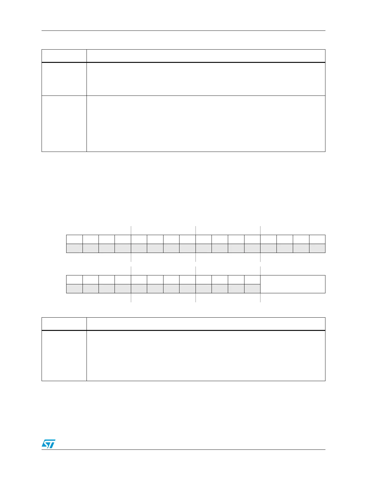
Figure 112. Interrupt Filter Maximum Counter registers 0–24 (IFMC[0:24])
Address:
Base + 0x1000 (IFMC0)
...
Base + 0x
1060
(IFMC24) 25 registers
Access: User read/write
0123456789101112131415
R000000 0000000 000
W
Reset0000000000000000
16 17 18 19 20 21 22 23 24 25 26 27 28 29 30 31
R 0 00000000000
MAXCNTx[3:0]
W
Reset0000000000000000
Table 108. IFMC[0:24] field descriptions
Field Description
MAXCNTx
[3:0]
Maximum Interrupt Filter Counter setting.
Filter Period = (T
CK
× MAXCNTx) +(n ×T
CK
)
Where n can be –2 to 3
MAXCNTx can be 0 to 15
T
CK
: Prescaled Filter Clock Period, which is IRC clock prescaled to IFCP value
T
IRC
: Basic Filter Clock Period: 62.5 ns (f
IRC
=16MHz)