RM0046 IEEE 1149.1 Test Access Port Controller (JTAGC)
Doc ID 16912 Rev 5 851/936
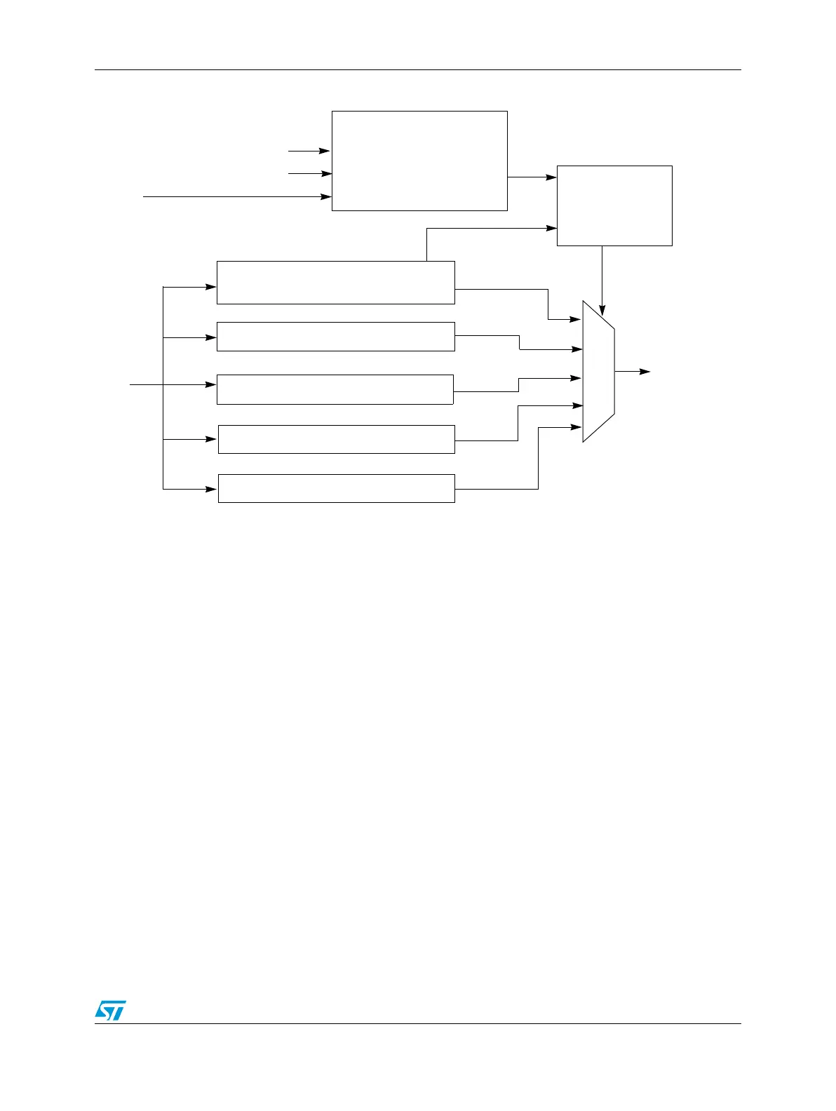
Figure 502. e200z0 OnCE block diagram
35.9.2 e200z0 OnCE controller functional description
The functional description for the e200z0 OnCE controller is the same as for the JTAGC,
with the differences described as follows.
Enabling the TAP controller
To access the e200z0 OnCE controller, the proper JTAGC instruction needs to be loaded in
the JTAGC instruction register, as discussed in Section , “TAP sharing mode. The e200z0
OnCE TAP controller may either be accessed independently or chained with the e200z1
OnCE TAP controller, such that the TDO output of the e200z1 TAP controller is fed into the
TDI input of the e200z0 TAP controller. The chained configuration allows commands to be
loaded into both core’s OnCE registers in one shift operation, so that both cores can be sent
a GO command at the same time for example.
35.9.3 e200z0 OnCE controller registers description
Most e200z0 OnCE debug registers are fully documented in the core reference manual.
OnCE Command register (OCMD)
The OnCE command register (OCMD) is a 10-bit shift register that receives its serial data
from the TDI pin and serves as the instruction register (IR). It holds the 10-bit commands to
be used as input for the e200z0 OnCE Decoder. The OCMD is shown in Figure 503. The
OCMD is updated when the TAP controller enters the update-IR state. It contains fields for
TCK
e200z0_TMS
TDI
Test Access Port (TAP)
e200z0_TDO
Bypass Register
External Data Register
Controller
TAP Instruction Register
OnCE Mapped Debug Registers
Auxiliary Data Register
e200z0_TRST
(OnCE OCMD)
TDO Mux
Control
{
From
JTAGC
(to JTAGC)