Clock Generation Module (MC_CGM) RM0046
124/936 Doc ID 16912 Rev 5
5.5.1 Output Clock Enable Register (CGM_OC_EN)
This register is used to enable and disable the output clock.
5.5.2 Output Clock Division Select Register (CGM_OCDS_SC)
This register is used to select the current output clock source and by which factor it is
divided before being delivered at the output clock.
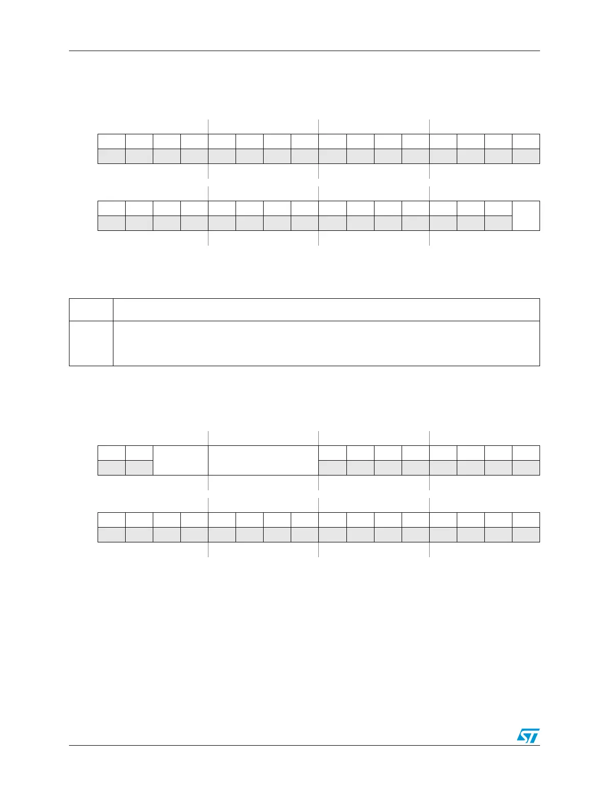
Figure 27. Output Clock Enable Register (CGM_OC_EN)
Address 0xC3FE_0370 Access: User read, Supervisor read/write, Test read/write
0123456789101112131415
R0000000000000000
W
Reset0000000000000000
16 17 18 19 20 21 22 23 24 25 26 27 28 29 30 31
R000000000000000
EN
W
Reset0000000000000000
Table 26. Output Clock Enable Register (CGM_OC_EN) Field Descriptions
Field Description
EN
Output Clock Enable control
0 Output Clock is disabled
1 Output Clock is enabled
Figure 28. Output Clock Division Select Register (CGM_OCDS_SC)
Address 0xC3FE_0374 Access: User read, Supervisor read/write, Test read/write
0123456789101112131415
R0 0
SELDIV SELCTL
00000000
W
Reset0000000000000000
16 17 18 19 20 21 22 23 24 25 26 27 28 29 30 31
R0000000000000000
W
Reset0000000000000000