Analog-to-Digital Converter (ADC) RM0046
582/936 Doc ID 16912 Rev 5
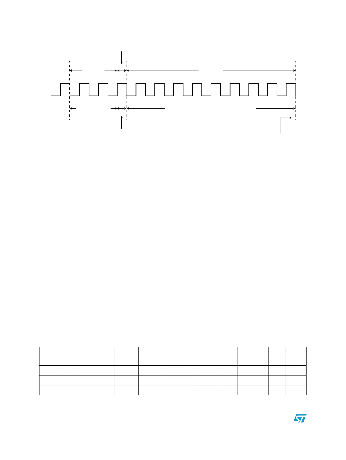
Figure 283. Sampling and conversion timings
The sampling phase duration is:
where ndelay is equal to 0.5 if INPSAMP is less than or equal to 06h, otherwise it is 1.
INPSAMP must be greater than or equal to 3 (hardware requirement).
The total evaluation phase duration is:
INPCMP must be greater than or equal to 1 and INPLATCH must be less than INCMP
(hardware requirements).
The total conversion duration is (not including external multiplexing):
The timings refer to the unit T
ck
, where f
ck
= (1/2 x ADC peripheral set clock).
0.5 cycles
2.5 cycles
Sampling phase Successive approximation / evaluation phase
10 cycles
Latching phase:
The capacitors field input
switch is opened
Note: Operating conditions — INPLATCH = 0, INPSAMP = 3, INPCMP = 1 and Fadc clk = 20 MHz
End of conversion
T
sample
INPSAMP ndelay–T
ck
=
T
eval
10 T
biteval
10 INPCMP T
ck
==
INPCMP 1 and INPLATCH INPCMP
T
conv
T
sample
T
eval
ndelay T
ck
++=
Table 290. ADC sampling and conversion timing at 5 V / 3.3 V for ADC0
Clock
(MHz)
T
ck
(s)
INPSAMPLE
(1)
Ndelay
(2)
T
sample
(3)
T
sample
/T
ck
INPCMP
T
eval
(s)
INPLATCH
T
conv
(s)
T
conv
/
T
ck
6 0.167 4 0.5 0.583 3.500 1 1.667 0 2.333 14.000
7 0.143 4 0.5 0.500 3.500 1 1.429 0 2.000 14.000
8 0.125 5 0.5 0.563 4.500 1 1.250 0 1.875 15.000