RM0046 Signal Description
Doc ID 16912 Rev 5 77/936
3.3.3 Pin multiplexing
Table 6 defines the pin list and muxing for the SPC560P40/34 devices.
Each row of Table 6 shows all the possible ways of configuring each pin, via alternate
functions. The default function assigned to each pin after reset is the ALT0 function.
SPC560P40/34 devices provide three main I/O pad types, depending on the associated
functions:
● Slow pads are the most common, providing a compromise between transition time and
low electromagnetic emission.
● Medium pads provide fast enough transition for serial communication channels with
controlled current to reduce electromagnetic emission.
● Fast pads provide maximum speed. They are used for improved NEXUS debugging
capability.
Medium and Fast pads can use slow configuration to reduce electromagnetic emission, at
the cost of reducing AC performance. For more information, see “Pad AC Specifications” in
the device datasheet.
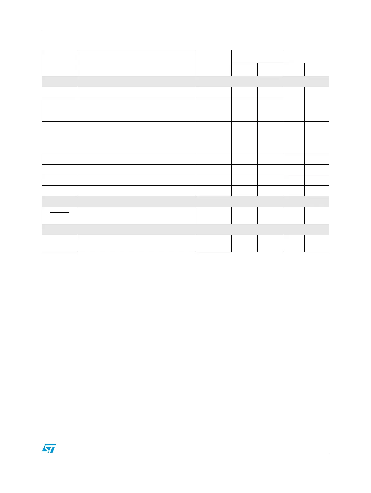
Table 5. System pins
Symbol Description Direction
Pad speed
(1)
Pin
SRC = 0 SRC = 1 64-pin 100-pin
Dedicated pins
NMI Non-maskable Interrupt Input only Slow — 1 1
XTAL
Analog output of the oscillator amplifier
circuit—needs to be grounded if oscillator is
used in bypass mode
———1118
EXTAL
Analog input of the oscillator amplifier circuit,
when the oscillator is not in bypass mode
Analog input for the clock generator when the
oscillator is in bypass mode
———1219
TDI JTAG test data input Input only Slow — 35 58
TMS JTAG state machine control Input only Slow — 36 59
TCK JTAG clock Input only Slow — 37 60
TDO JTAG test data output Output only Slow Fast 38 61
Reset pin
RESET
Bidirectional reset with Schmitt trigger
characteristics and noise filter
Bidirectional Medium — 13 20
Test pin
VPP_TEST
Pin for testing purpose only. To be tied to
ground in normal operating mode.
———4774
1. SRC values refer to the value assigned to the Slew Rate Control bits of the pad configuration register.