Deserial Serial Peripheral Interface (DSPI) RM0046
470/936 Doc ID 16912 Rev 5
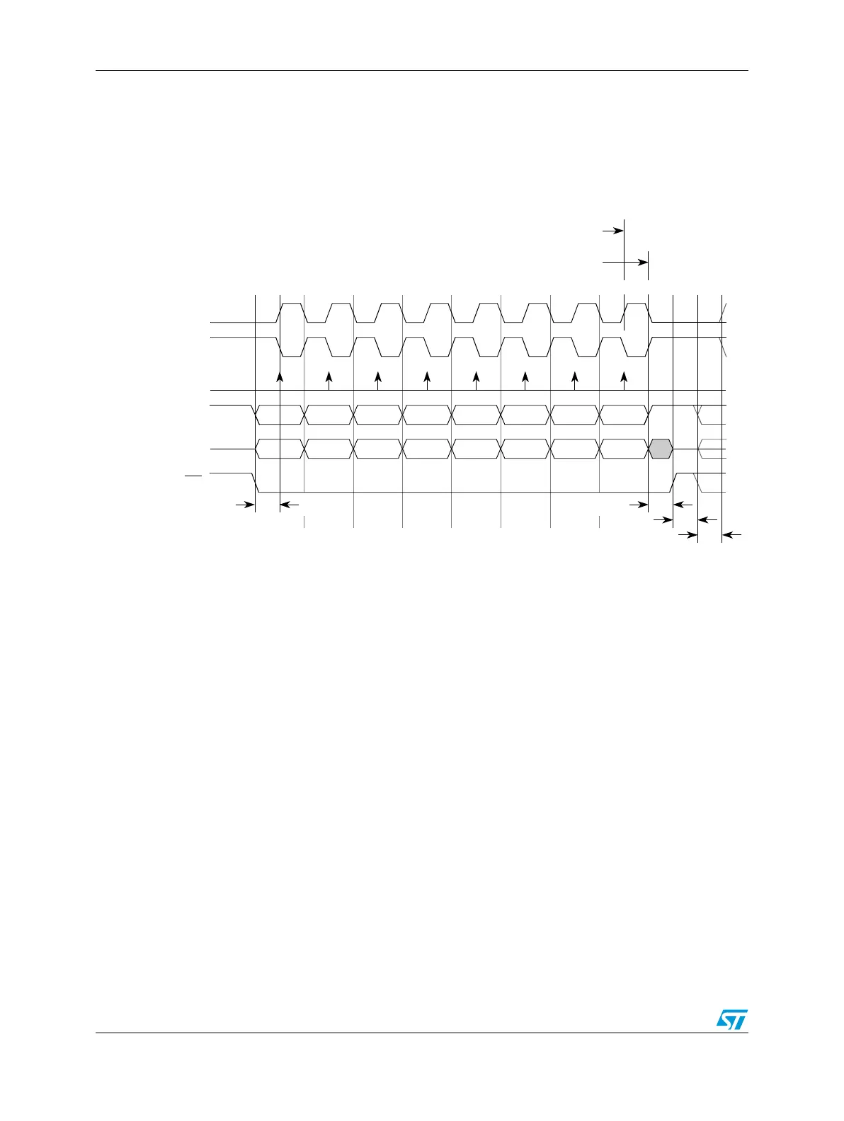
Classic SPI transfer format (CPHA = 0)
The transfer format shown in Figure 220 is used to communicate with peripheral SPI slave
devices where the first data bit is available on the first clock edge. In this format, the master
and slave sample their SIN_x pins on the odd-numbered SCK_x edges and change the data
on their SOUT_x pins on the even-numbered SCK_x edges.
Figure 220. DSPI transfer timing diagram (MTFE = 0, CPHA = 0, FMSZ = 8)
The master initiates the transfer by placing its first data bit on the SOUT_x pin and asserting
the appropriate peripheral chip select signals to the slave device. The slave responds by
placing its first data bit on its SOUT_x pin. After the t
CSC
delay has elapsed, the master
outputs the first edge of SCK_x. This is the edge used by the master and slave devices to
sample the first input data bit on their serial data input signals. At the second edge of the
SCK_x the master and slave devices place their second data bit on their serial data output
signals. For the rest of the frame the master and the slave sample their SIN_x pins on the
odd-numbered clock edges and changes the data on their SOUT_x pins on the even-
numbered clock edges. After the last clock edge occurs a delay of t
ASC
is inserted before the
master negates the CS signals. A delay of t
DT
is inserted before a new frame transfer can be
initiated by the master.
For the CPHA = 0 condition of the master, TCF and EOQF are set and the RXCTR counter
is updated at the next to last serial clock edge of the frame (edge 15) of Figure 220.
For the CPHA = 0 condition of the slave, TCF is set and the RXCTR counter is updated at
the last serial clock edge of the frame (edge 16) of Figure 220.
SCK
(CPOL = 0)
PCSx / SS
t
ASC
SCK
(CPOL = 1)
Master and slave
sample
Master SOUT /
Slave SIN
Master SIN /
Slave SOUT
Bit 6
Bit 1
Bit 5
Bit 2
Bit 4
Bit 3
Bit 3
Bit 4
Bit 2
Bit 5
Bit 1
Bit 6
LSB
MSB
MSB
LSB
t
DT
t
CSC
t
CSC
MSB first (LSBFE = 0):
LSB first (LSBFE = 1):
t
CSC
= CSCS to SCK delay.
t
ASC
= After SCK delay.
t
DT
= Delay after transfer (minimum CS idle time).
Master (CPHA = 0): TCF and EOQF are set and RXCTR counter
is updated at next to last SCK edge of frame (edge 15)
Slave (CPHA = 0): TCF is set and RXCTR counter is updated at
last SCK edge of frame (edge 16)
1234567891011121314 1615