RM0046 Flash Memory
Doc ID 16912 Rev 5 311/936
17 Flash Memory
17.1 Introduction
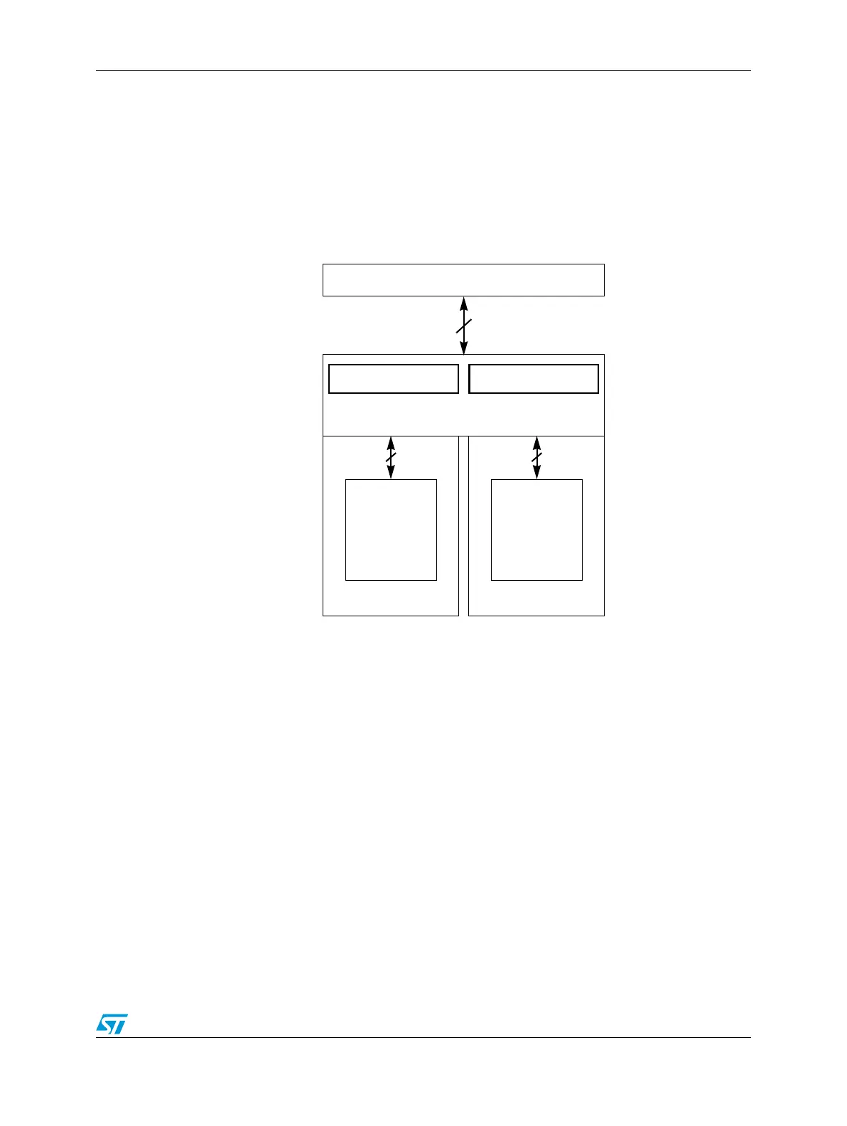
The Flash memory comprises a platform Flash controller interface and two Flash memory
arrays: one array of 256 KB for code (code Flash) and one array of 64 KB for data (data
Flash). The Flash architecture of the SPC560P40/34 device is illustrated in Figure 144.
Figure 144. SPC560P40/34 Flash memory architecture
17.2 Platform Flash controller
17.2.1 Introduction
This section provides an introduction of the platform Flash controller, which acts as the
interface between the system bus and as many as two banks of Flash memory arrays
(program and data). It intelligently converts the protocols between the system bus and the
dedicated Flash array interfaces. Several important terms are used to describe the platform
Flash controller module and its connections. These terms are defined here.
● Port—This term describes the AMBA-AHB connection(s) into the platform Flash
controller. From an architectural and programming model viewpoint, the definition
supports as many as two AHB ports, even though this specific controller only supports
a single AHB connection.
● Bank—This term describes the attached Flash memories. From the platform Flash
controller’s perspective, there may be one or two attached banks of Flash memory. The
code Flash bank is required and always attached to bank0. Additionally, there is a data
Flash attached to bank1. The platform Flash controller interface supports two separate
AHB CROSSBAR SWITCH
Bank0 (code Flash) Bank1 (data Flash)
AHB ports 32
64 KB
Array 0Array 0
1x128 Page Buffer4x128 Page Buffer
PFlash Controller
Data Flash Code Flash
256 KB