Deserial Serial Peripheral Interface (DSPI) RM0046
468/936 Doc ID 16912 Rev 5
Delay after transfer (t
DT
)
The delay after transfer is the length of time between negation of the CSx signal for a frame
and the assertion of the CS
x signal for the next frame. The PDT and DT fields in the
DSPIx_CTARn registers select the delay after transfer.
Refer to Figure 220 for an illustration of the delay after transfer.
The following formula expresses the PDT/DT/delay after transfer relationship:
Equation 24
Table 225 shows an example of the computed delay after transfer.
Peripheral Chip Select strobe enable (CS5_x)
The CS5_x signal provides a delay to allow the CSx signals to settle after transitioning,
thereby avoiding glitches. When the DSPI is in master mode and PCSSE bit is set in the
DSPIx_MCR, CS5_x provides a signal for an external demultiplexer to decode the CS4_x
signals into as many as 32 glitch-free CSx signals.
Figure 219 shows the timing of the CS5_x signal relative to CS signals.
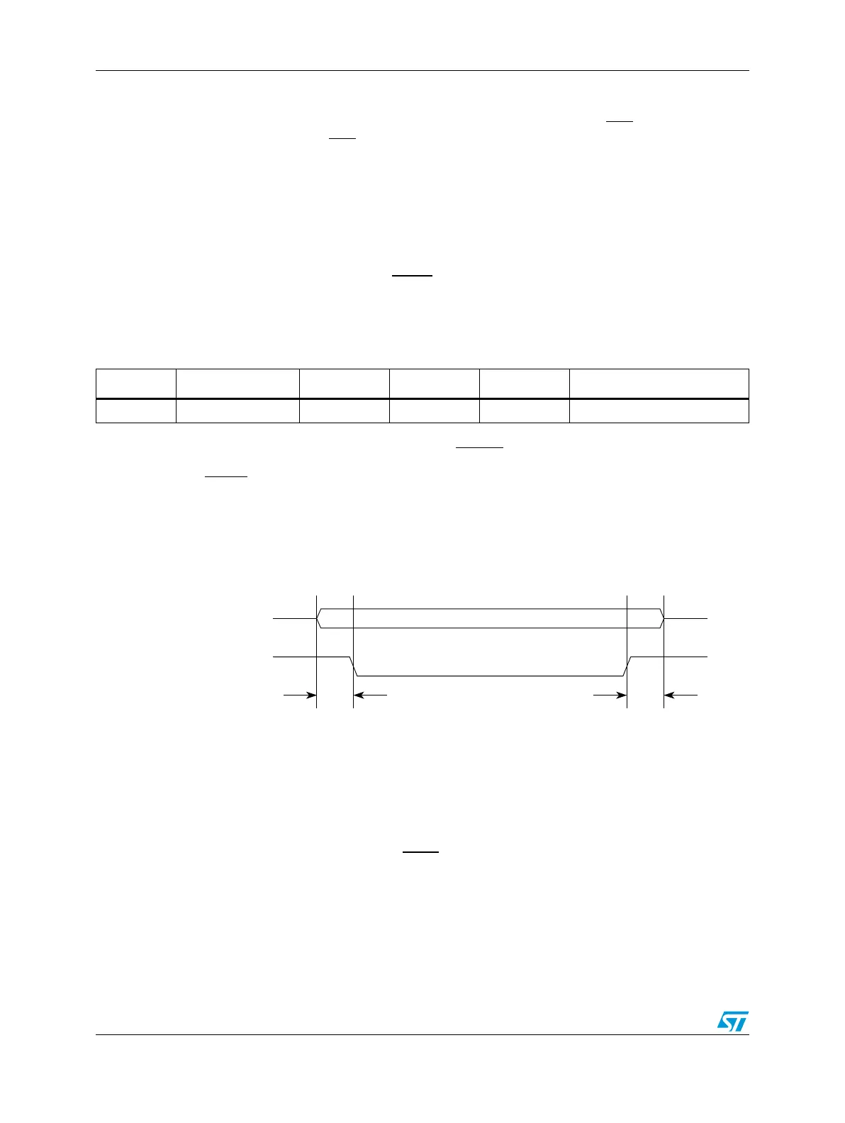
Figure 219. Peripheral Chip Select strobe timing
The delay between the assertion of the CSx signals and the assertion of CS5_x signal is
selected by the PCSSCK field in the DSPIx_CTAR based on the following formula:
Equation 25
At the end of the transfer the delay between CS5_x negation and CSx negation is selected
by the PASC field in the DSPIx_CTAR based on the following formula:
Table 225. Delay after transfer computation example
PDT Prescaler value DT Scaler value f
SYS
Delay after transfer
0b01 3 0b1110 32768 100 MHz 0.98 ms