RM0046 Flash Memory
Doc ID 16912 Rev 5 329/936
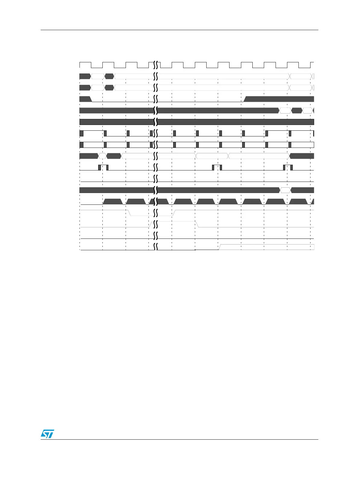
Figure 150. 3-cycle access, terminate-and-retry with BKn_RWWC = 10x
Figure 150 shows the terminate-while-write timing diagram. In this example, the 3-cycle
access to address y is interrupted when an operation causes the bkn_done signal to be
negated, signaling that the array bank is busy with a high-voltage program or erase event.
Based on the setting of BKn_RWWC, once the bkn_done signal is detected as negated, the
platform Flash controller asserts bkn_abort, which forces the Flash array to cancel the high-
voltage program or erase event. The array operation completes (at the end of cycle 4) and
bkn_done returns to a logical 1. It should be noted that the time spent in cycle 4 for
Figure 150 is considerably less than the time in the same cycle in Figure 149 (because of
the terminate operation). In cycle 6, the platform Flash controller module retries the read to
address y that was interrupted by the negation of bkn_done in cycle 3. Note that throughout
cycles 2–9, the AHB bus pipeline is stalled with a read to address y in the AHB data phase
and a read to address y+4 in the address phase. Depending on the state of the least-
significant-bit of the BKn_RWWC control field, the hardware may also signal an termination
notification interrupt (if BKn_RWWC = 100). The stall notification interrupt is shown as the
optional assertion of ECSM’s MIR[FBnAI] (Flash bank n termination interrupt).
nonseq
seq
addr y
addr y+4
C(y)
C(y+4)
okay okay okay okay okay okay okay okay
y
C(y)
Burst Read, Abort-and-Retry, APC = 2, RWSC = 2, PFLM = 2
123456
78
addr y
seq
addr y+8
y+16 y+16
y
okay okay
addr y+16addr y (retry)
hclk
htrans
haddr, hprot
hwrite
hrdata
hwdata
hready_out
hresp
bkn_fl_addr
bkn_fl_rd_en
bkn_fl_wr_en
bkn_fl_rdata
bkn_fl_xfr_err
bkn_done
bkn_abort
ecsm_mir[fbnsi]
ecsm_mir[fbnai]
9
10