System Integration Unit Lite (SIUL) RM0046
262/936 Doc ID 16912 Rev 5
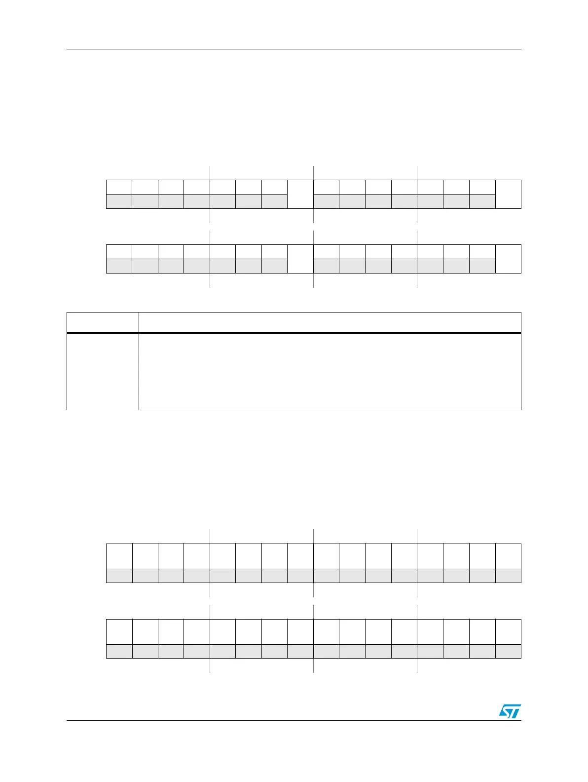
GPIO Pad Data Output registers 0_3–68_71 (GPDO[0_3:68_71])
These registers can be used to set or clear a single GPIO pad with a byte access.
GPIO Pad Data Input registers 0_3–68_71 (GPDI[0_3:68_71])
These registers can be used to read the GPIO pad data with a byte access.
Figure 107. Port GPIO Pad Data Output registers 0_3–68_71 (GPDO[0_3:68_71])
Address:
Base + 0x0600 (GPDO0_3)
...
Base + 0x0644 (GPDO68_71) 18 registers
Access: User read/write
0123456789101112131415
R000000 0
PDO
[0]
00000 00
PDO
[1]
W
Reset0000000000000000
16 17 18 19 20 21 22 23 24 25 26 27 28 29 30 31
R 0 000000
PDO
[2]
0 000000
PDO
[3]
W
Reset0000000000000000
Table 103. GPDO[0_3:68_71] field descriptions
Field Description
PDO[n]
Pad Data Out
This bit stores the data to be driven out on the external GPIO pad controlled by this register.
0: Logic low value is driven on the corresponding GPIO pad when the pad is configured as an
output.
1: Logic high value is driven on the corresponding GPIO pad when the pad is configured as an
output.
Figure 108. GPIO Pad Data Input registers 0_3–68_71 (GPDI[0_3:68_71])
Address:
Base + 0x0800 (GPDI0_3)
...
Base + 0x0844 (GPDI68_71) 18 registers
Access: User read-only
0123456789101112131415
R000000 0
PDI
[0]
0000000
PDI
[1]
W
Reset0000000000000000
16 17 18 19 20 21 22 23 24 25 26 27 28 29 30 31
R 0 000000
PDI
[2]
0000000
PDI
[3]
W
Reset0000000000000000