RM0046 Reset Generation Module (MC_RGM)
Doc ID 16912 Rev 5 195/936
Note: The F_POR flag is automatically cleared on a 1.2 V low-voltage detected or a 2.7 V low-
voltage detected. This means that if the power-up sequence is not monotonic (i.e., the
voltage rises and then drops enough to trigger a low-voltage detection), the F_POR flag may
not be set but instead the <register>F_LVD12 or <register>F_LVD27_VREG flag is set on
exiting the reset sequence. Therefore, if the F_POR, <register>F_LVD12 or
<register>F_LVD27_VREG flags are set on reset exit, software should interpret the reset
cause as power-on.
Functional Event Reset Disable Register (RGM_FERD)
This register provides dedicated bits to disable functional reset sources.When a functional
reset source is disabled, the associated functional event will trigger either a SAFE mode
request or an interrupt request (see Section , “Functional Event Alternate Request Register
(RGM_FEAR)). It can be accessed in read/write in either supervisor mode or test mode. It
can be accessed in read only in user mode. Each byte can be written only once after power-
on reset.
F_LVD27_VREG
Flag for 2.7V low-voltage detected (VREG)
0 No 2.7V low-voltage detected (VREG) event has occurred since either the last clear or the last
power-on reset assertion
1 A 2.7V low-voltage detected (VREG) event has occurred
F_SWT
Flag for software watchdog timer
0 No software watchdog timer event has occurred since either the last clear or the last power-
on reset assertion
1 A software watchdog timer event has occurred
F_LVD12
Flag for 1.2V low-voltage detected
0 No 1.2V low-voltage detected event has occurred since either the last clear or the last power-
on reset assertion
1 A 1.2V low-voltage detected event has occurred
Table 59. Destructive Event Status Register (RGM_DES) Field Descriptions (continued)
Field Description
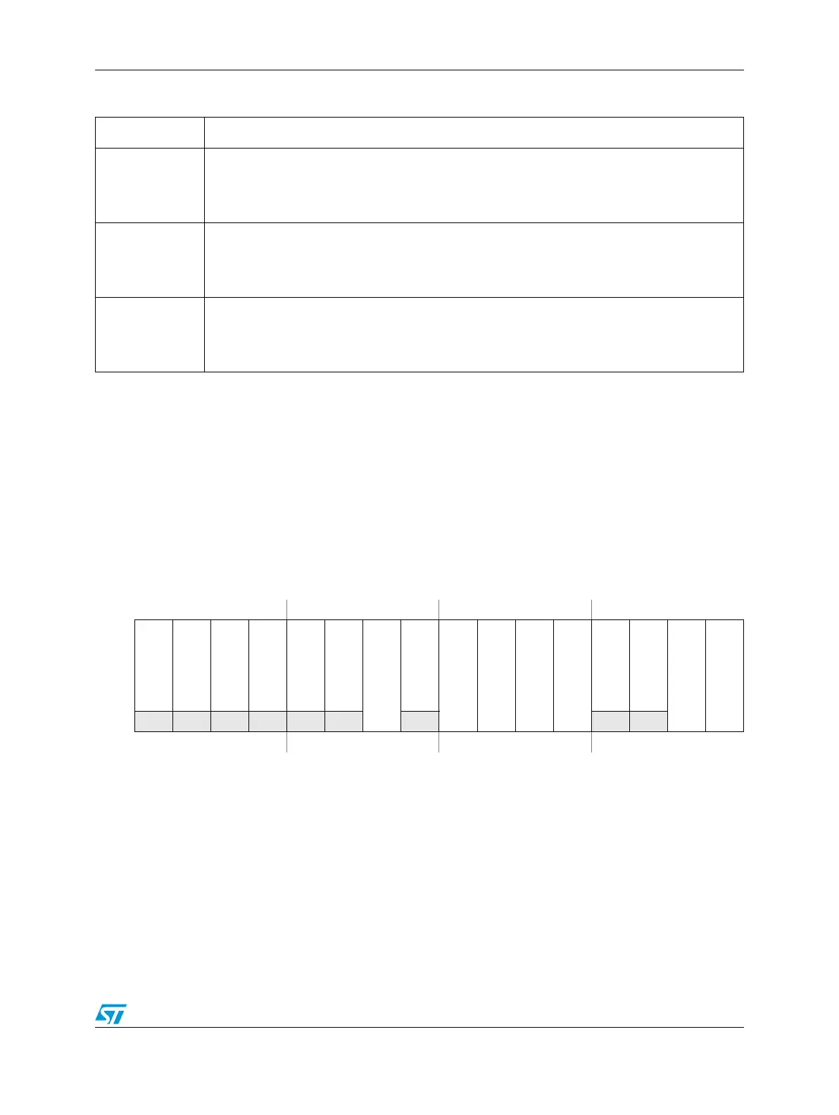
Figure 71. Functional Event Reset Disable Register (RGM_FERD)
Address 0xC3FE_4004 Access: User read, Supervisor read/write, Test read/write
0123456789101112131415
R
D_EXR
00000
D_PLL1
D_FLASH
D_LVD45
D_CMU0_FHL
D_CMU0_OLR
D_PLL0
D_CHKSTOP
D_SOFT
D_CORE
D_JTAG
W
POR0000000000000000