■ Converter uses signals VREFA+ and GNDA as the voltage reference
■ Power and ground for the analog circuitry is separate from the digital power and ground
■ Efficient transfers using Micro Direct Memory Access Controller (µDMA)
– Dedicated channel for each sample sequencer
– ADC module uses burst requests for DMA
■ Global Alternate Clock (ALTCLK) resource or System Clock (SYSCLK) can be used to generate
ADC clock
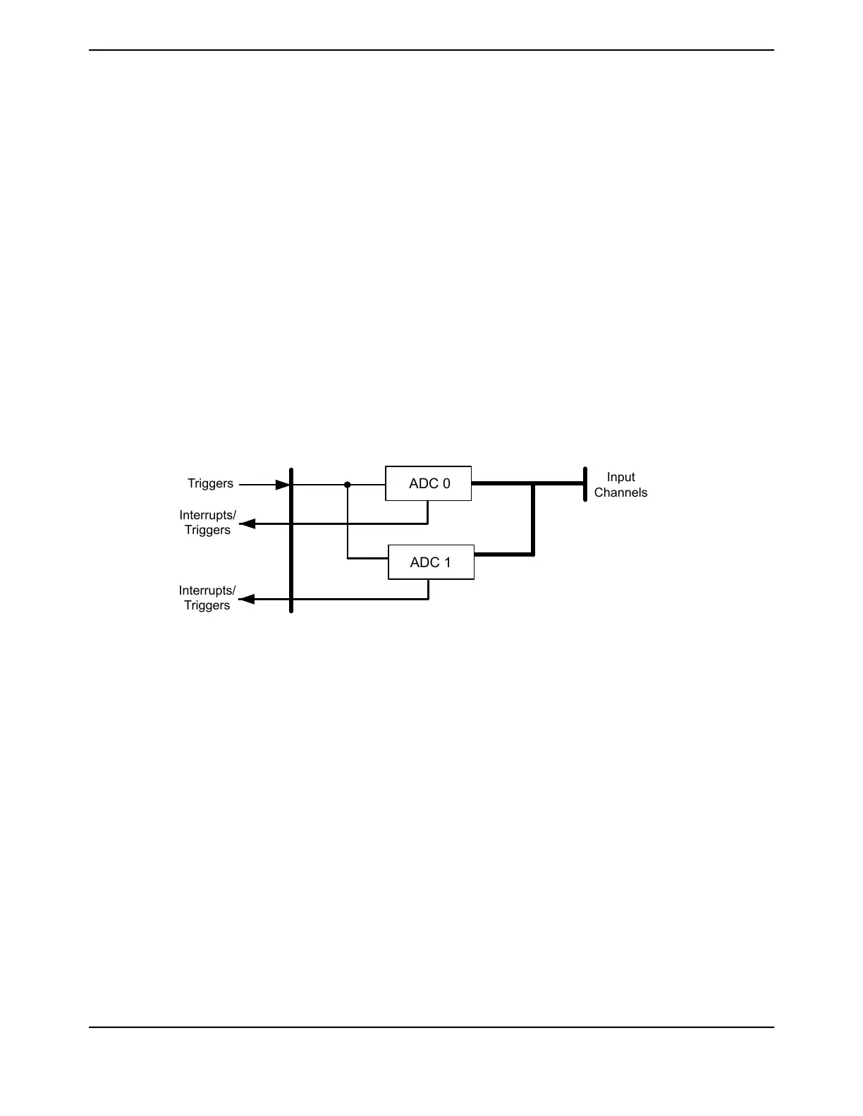
15.1 Block Diagram
The TM4C1294NCPDT microcontroller contains two identical Analog-to-Digital Converter modules.
These two modules, ADC0 and ADC1, share the same 20 analog input channels. Each ADC module
operates independently and can therefore execute different sample sequences, sample any of the
analog input channels at any time, and generate different interrupts and triggers. Figure
15-1 on page 1054 shows how the two modules are connected to analog inputs and the system bus.
Figure 15-1. Implementation of Two ADC Blocks
Input
Channels
Triggers
Interrupts/
Triggers
ADC 0
ADC 1
Interrupts/
Triggers
Figure 15-2 on page 1055 provides details on the internal configuration of the ADC controls and data
registers.
June 18, 20141054
Texas Instruments-Production Data
Analog-to-Digital Converter (ADC)
 Loading...


