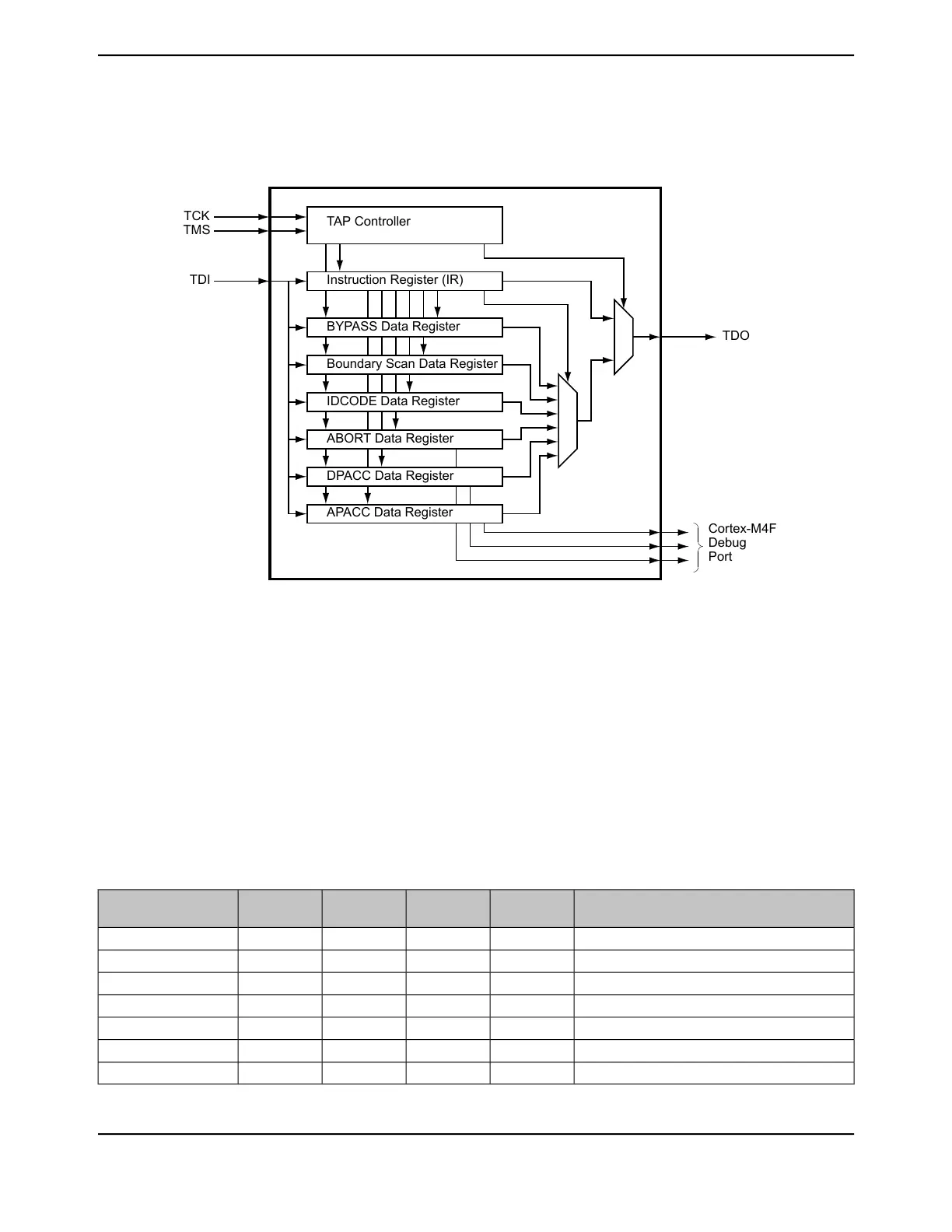
4.1 Block Diagram
Figure 4-1. JTAG Module Block Diagram
Instruction Register (IR)
TAP Controller
BYPASS Data Register
Boundary Scan Data Register
IDCODE Data Register
ABORT Data Register
DPACC Data Register
APACC Data Register
TCK
TMS
TDI
TDO
Cortex-M4F
Debug
Port
4.2 Signal Description
The following table lists the external signals of the JTAG/SWD controller and describes the function
of each. The JTAG/SWD controller signals are alternate functions for some GPIO signals, however
note that the reset state of the pins is for the JTAG/SWD function. The JTAG/SWD controller signals
are under commit protection and require a special process to be configured as GPIOs, see “Commit
Control” on page 752. The column in the table below titled "Pin Mux/Pin Assignment" lists the GPIO
pin placement for the JTAG/SWD controller signals. The AFSEL bit in the GPIO Alternate Function
Select (GPIOAFSEL) register (page 770) is set to choose the JTAG/SWD function. The number in
parentheses is the encoding that must be programmed into the PMCn field in the GPIO Port Control
(GPIOPCTL) register (page 787) to assign the JTAG/SWD controller signals to the specified GPIO
port pin. For more information on configuring GPIOs, see “General-Purpose Input/Outputs
(GPIOs)” on page 742.
Table 4-1. JTAG_SWD_SWO Signals (128TQFP)
DescriptionBuffer TypePin TypePin Mux / Pin
Assignment
Pin NumberPin Name
JTAG/SWD CLK.TTLIPC0 (1)100SWCLK
JTAG TMS and SWDIO.TTLI/OPC1 (1)99SWDIO
JTAG TDO and SWO.TTLOPC3 (1)97SWO
JTAG/SWD CLK.TTLIPC0 (1)100TCK
JTAG TDI.TTLIPC2 (1)98TDI
JTAG TDO and SWO.TTLOPC3 (1)97TDO
JTAG TMS and SWDIO.TTLIPC1 (1)99TMS
June 18, 2014208
Texas Instruments-Production Data
JTAG Interface
 Loading...


