pair 1 samples analog inputs 2 and 3; and so on (see Table 15-6 on page 1066). The ADC does not
support other differential pairings such as analog input 0 with analog input 3.
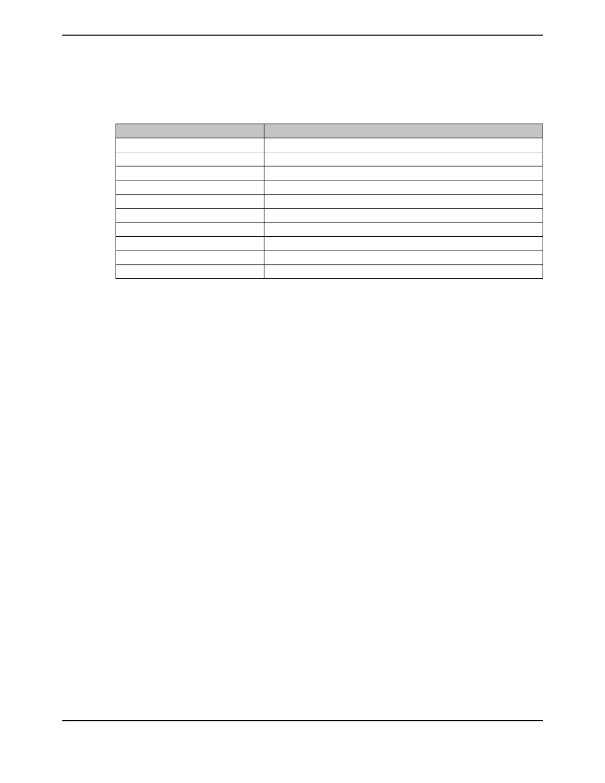
Table 15-6. Differential Sampling Pairs
Analog InputsDifferential Pair
0 and 10
2 and 31
4 and 52
6 and 73
8 and 94
10 and 115
12 and 136
14 and 157
16 and 178
18 and 199
The voltage sampled in differential mode is the difference between the odd and even channels:
■ Input Positive Voltage: VIN+ = V
IN_EVEN
(even channel)
■ Input Negative Voltage: VIN- = V
IN_ODD
(odd channel)
The input differential voltage is defined as: VIN
D
= VIN+ - VIN-, therefore:
■ If VIN
D
= 0, then the conversion result = 0x800
■ If VIN
D
> 0, then the conversion result > 0x800 (range is 0x800–0xFFF)
■ If VIN
D
< 0, then the conversion result < 0x800 (range is 0–0x800)
When using differential sampling, the following definitions are relevant:
■ Input Common Mode Voltage: VIN
CM
= (VIN+ + VIN-) / 2
■ Reference Positive Voltage: VREFP
■ Reference Negative Voltage: VREFN
■ Reference Differential Voltage: VREF
D
= VREFP - VREFN
■ Reference Common Mode Voltage: VREF
CM
= (VREFP + VREFN) / 2
The following conditions provide optimal results in differential mode:
■ Both V
IN_EVEN
and V
IN_ODD
must be in the range of (VREFP to VREFN) for a valid conversion
result
■ The maximum possible differential input swing, or the maximum differential range, is: -VREF
D
to
+VREF
D
, so the maximum peak-to-peak input differential signal is (+VREF
D
- -VREF
D
) = 2 *
VREF
D
= 2 * (VREFP - VREFN)
June 18, 20141066
Texas Instruments-Production Data
Analog-to-Digital Converter (ADC)
 Loading...


