Register 29: ADC Sample Sequence Input Multiplexer Select 1 (ADCSSMUX1),
offset 0x060
Register 30: ADC Sample Sequence Input Multiplexer Select 2 (ADCSSMUX2),
offset 0x080
This register, along with the ADCSSEMUX1 or ADCSSEMUX2 register, defines the analog input
configuration for each sample in a sequence executed with Sample Sequencer 1 or 2. If the
corresponding EMUXn bit in the ADCSSEMUX1 or ADCSSEMUX2 register is set, the MUXn field in
this register selects from AIN[19:16]. When the corresponding EMUXn bit is clear, the MUXn field
selects from AIN[15:0]. These registers are 16 bits wide and contain information for four possible
samples. See the ADCSSMUX0 register on page 1109 for detailed bit descriptions. The ADCSSMUX1
register affects Sample Sequencer 1 and the ADCSSMUX2 register affects Sample Sequencer 2.
Note: Channels AIN[31:20] do not exist on this microcontroller. Configuring MUXn to be 0xC-0xF
when the corresponding EMUXn bit is set results in undefined behavior.
ADC Sample Sequence Input Multiplexer Select n (ADCSSMUXn)
ADC0 base: 0x4003.8000
ADC1 base: 0x4003.9000
Offset 0x060
Type RW, reset 0x0000.0000
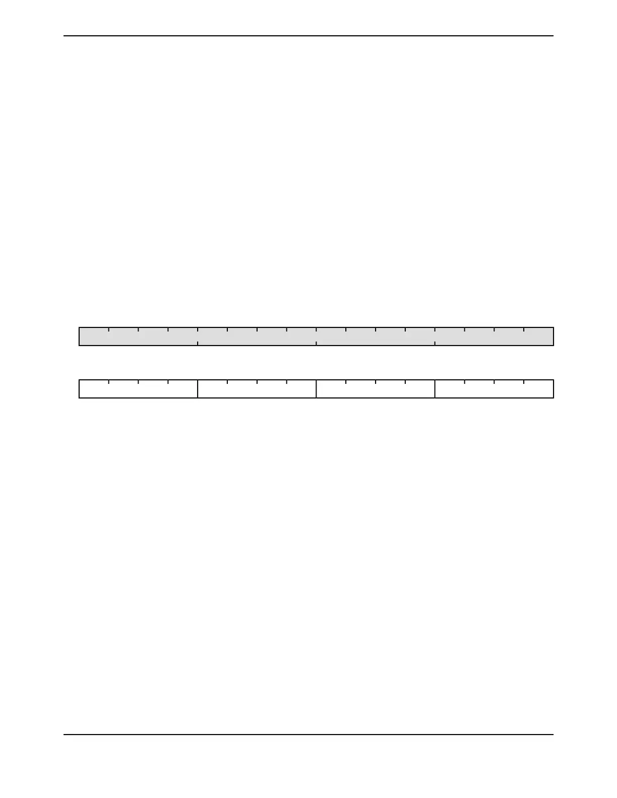
16171819202122232425262728293031
reserved
ROROROROROROROROROROROROROROROROType
0000000000000000Reset
0123456789101112131415
MUX0MUX1MUX2MUX3
RWRWRWRWRWRWRWRWRWRWRWRWRWRWRWRWType
0000000000000000Reset
DescriptionResetTypeNameBit/Field
Software should not rely on the value of a reserved bit. To provide
compatibility with future products, the value of a reserved bit should be
preserved across a read-modify-write operation.
0x0000ROreserved31:16
4th Sample Input Select0x0RWMUX315:12
3rd Sample Input Select0x0RWMUX211:8
2nd Sample Input Select0x0RWMUX17:4
1st Sample Input Select0x0RWMUX03:0
1129June 18, 2014
Texas Instruments-Production Data
Tiva
™
TM4C1294NCPDT Microcontroller
 Loading...


