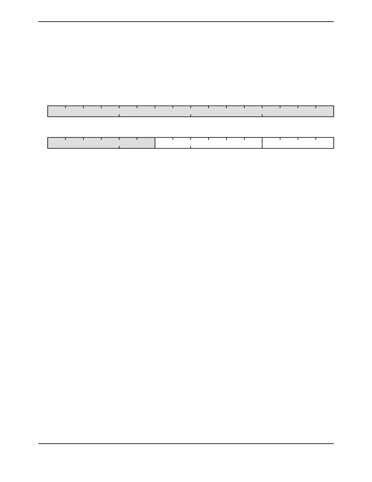
Register 66: ADC Clock Configuration (ADCCC), offset 0xFC8
The ADCCC register controls the clock source for the ADC module.
ADC Clock Configuration (ADCCC)
ADC0 base: 0x4003.8000
ADC1 base: 0x4003.9000
Offset 0xFC8
Type RW, reset 0x0000.0001
16171819202122232425262728293031
reserved
ROROROROROROROROROROROROROROROROType
0000000000000000Reset
0123456789101112131415
CSCLKDIVreserved
RWRWRWRWRWRWRWRWRWRWROROROROROROType
1000000000000000Reset
DescriptionResetTypeNameBit/Field
Software should not rely on the value of a reserved bit. To provide
compatibility with future products, the value of a reserved bit should be
preserved across a read-modify-write operation.
0x0000.00ROreserved31:10
PLL VCO Clock Divisor
DescriptionValue
/10x0
/20x1
/30x2
/(N + 1)0xN
0x0RWCLKDIV9:4
ADC Clock Source
DescriptionValue
PLL VCO divided by CLKDIV.0x0
Alternate clock source as defined by ALTCLKCFG register
in System Control Module.
0x1
MOSC0x2
Reserved0x2 - 0xF
0x1RWCS3:0
June 18, 20141160
Texas Instruments-Production Data
Analog-to-Digital Converter (ADC)
 Loading...


