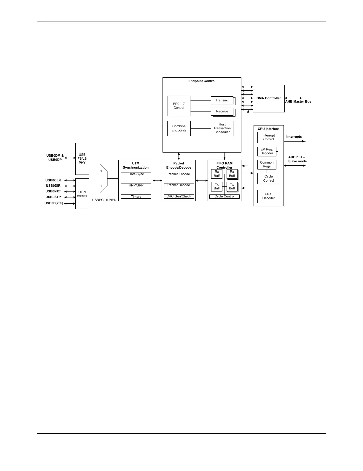
21.1 Block Diagram
Figure 21-1. USB Module Block Diagram
Packet
Encode/Decode
Endpoint Control
EP0 – 7
Control
Transmit
Receive
Combine
Endpoints
Host
Transaction
Scheduler
Packet Encode
Packet Decode
CRC Gen/Check
FIFO RAM
Controller
Cycle Control
Rx
Buff
Rx
Buff
Tx
Buff
Tx
Buff
CPU Interface
Interrupt
Control
EP Reg.
Decoder
Common
Regs
Cycle
Control
FIFO
Decoder
Interrupts
AHB bus –
Slave mode
UTM
Synchronization
Data Sync
HNP/SRP
Timers
USB0DM &
USB0DP
DMA Controller
USB
FS/LS
PHY
0
1
ULPI
Interface
USBPC.ULPIEN
USB0DIR
USB0NXT
USB0STP
USB0CLK
USB0D[7:0]
AHB Master Bus
21.2 Signal Description
The following table lists the external signals of the USB controller and describes the function of
each. Some USB controller signals are alternate functions for some GPIO signals and default to be
GPIO signals at reset. The column in the table below titled "Pin Mux/Pin Assignment" lists the
possible GPIO pin placements for these USB signals. The AFSEL bit in the GPIO Alternate Function
Select (GPIOAFSEL) register (page 770) should be set to choose the USB function. The number in
parentheses is the encoding that must be programmed into the PMCn field in the GPIO Port Control
(GPIOPCTL) register (page 787) to assign the USB signal to the specified GPIO port pin. The
USB0VBUS and USB0ID signals are configured by clearing the appropriate DEN bit in the GPIO
Digital Enable (GPIODEN) register. For more information on configuring GPIOs, see
“General-Purpose Input/Outputs (GPIOs)” on page 742. The remaining signals (with the word "fixed"
in the Pin Mux/Pin Assignment column) have a fixed pin assignment and function.
Note: When used in OTG mode, USB0VBUS and USB0ID do not require any configuration as they
are dedicated pins for the USB controller and directly connect to the USB connector's VBUS
and ID signals. If the USB controller is used as either a dedicated Host or Device, the
DEVMOD field in the USB General-Purpose Control and Status (USBGPCS) register can
be used to connect the USB0VBUS and/or USB0ID inputs to fixed levels internally, freeing
the PB0 and PB1 pins for GPIO use. Note that PB1 (USB0VBUS) is a 5-V tolerant signal as
required. For proper self-powered Device operation, the VBUS value must still be monitored
to assure that if the Host removes VBUS, the self-powered Device disables the D+/D- pull-up
resistors. This function can be accomplished by connecting a standard GPIO to VBUS.
The termination resistors for the USB PHY have been added internally, and thus there is
no need for external resistors. For a device, there is a 1.5 KOhm pull-up on the D+ and for
a host there are 15 KOhm pull-downs on both D+ and D-.
1645June 18, 2014
Texas Instruments-Production Data
Tiva
™
TM4C1294NCPDT Microcontroller
 Loading...


