Register 3: Flash Memory Control (FMC), offset 0x008
When this register is written, the Flash memory controller initiates the appropriate access cycle for
the location specified by the Flash Memory Address (FMA) register (see page 625). If the access
is a write access, the data contained in the Flash Memory Data (FMD) register (see page 626) is
written to the specified address.
For non-volatile registers, FMPREn, FMPPEn, USER_REGn, and USER_REGn, the respective
register is programmed with the value to be written rather than the FMD register.
This register must be the final register written and initiates the memory operation. The four control
bits in the lower byte of this register are used to initiate memory operations.
Care must be taken not to set multiple control bits as the results of such an operation are
unpredictable.
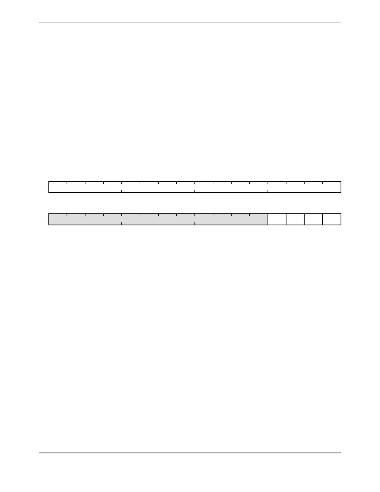
Flash Memory Control (FMC)
Base 0x400F.D000
Offset 0x008
Type RW, reset 0x0000.0000
16171819202122232425262728293031
WRKEY
WOWOWOWOWOWOWOWOWOWOWOWOWOWOWOWOType
0000000000000000Reset
0123456789101112131415
WRITEERASEMERASECOMTreserved
RWRWRWRWROROROROROROROROROROROROType
0000000000000000Reset
DescriptionResetTypeNameBit/Field
Flash Memory Write Key
This field contains a write key, which is used to minimize the incidence
of accidental Flash memory writes. The value 0xA442 or the PEKEY
value in the FLPEKEY register must be written into this field for a Flash
memory write to occur. The use of 0xA442 or PEKEY is dependent on
the value of the KEY bit in the BOOTCFG register at 0x1D0.
Writes to the FMC register without this WRKEY value are ignored. A read
of this field returns the value 0.
0x0000WOWRKEY31:16
Software should not rely on the value of a reserved bit. To provide
compatibility with future products, the value of a reserved bit should be
preserved across a read-modify-write operation.
0x00ROreserved15:4
627June 18, 2014
Texas Instruments-Production Data
Tiva
™
TM4C1294NCPDT Microcontroller
 Loading...


