Register 24: GPIO DMA Control (GPIODMACTL), offset 0x534
This register is used to configure a GPIO pin as a source for the μDMA trigger.
GPIO DMA Control (GPIODMACTL)
GPIO Port A (AHB) base: 0x4005.8000
GPIO Port B (AHB) base: 0x4005.9000
GPIO Port C (AHB) base: 0x4005.A000
GPIO Port D (AHB) base: 0x4005.B000
GPIO Port E (AHB) base: 0x4005.C000
GPIO Port F (AHB) base: 0x4005.D000
GPIO Port G (AHB) base: 0x4005.E000
GPIO Port H (AHB) base: 0x4005.F000
GPIO Port J (AHB) base: 0x4006.0000
GPIO Port K (AHB) base: 0x4006.1000
GPIO Port L (AHB) base: 0x4006.2000
GPIO Port M (AHB) base: 0x4006.3000
GPIO Port N (AHB) base: 0x4006.4000
GPIO Port P (AHB) base: 0x4006.5000
GPIO Port Q (AHB) base: 0x4006.6000
Offset 0x534
Type RW, reset 0x0000.0000
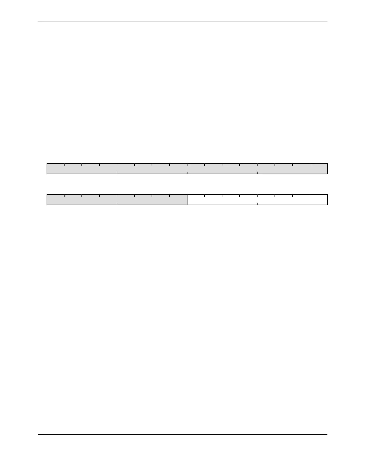
16171819202122232425262728293031
reserved
ROROROROROROROROROROROROROROROROType
0000000000000000Reset
0123456789101112131415
DMAENreserved
RWRWRWRWRWRWRWRWROROROROROROROROType
0000000000000000Reset
DescriptionResetTypeNameBit/Field
Software should not rely on the value of a reserved bit. To provide
compatibility with future products, the value of a reserved bit should be
preserved across a read-modify-write operation.
0x0000.00ROreserved31:8
μDMA Trigger Enable
DescriptionValue
The corresponding pin is not used to trigger the μDMA.0
The corresponding pin is used to trigger the μDMA.1
0x00RWDMAEN7:0
June 18, 2014790
Texas Instruments-Production Data
General-Purpose Input/Outputs (GPIOs)
 Loading...


