Note: The following pins are configured as JTAG port pins out of reset. Refer to “General-Purpose
Input/Outputs (GPIOs)” on page 742 for information on how to reprogram the configuration
of these pins.
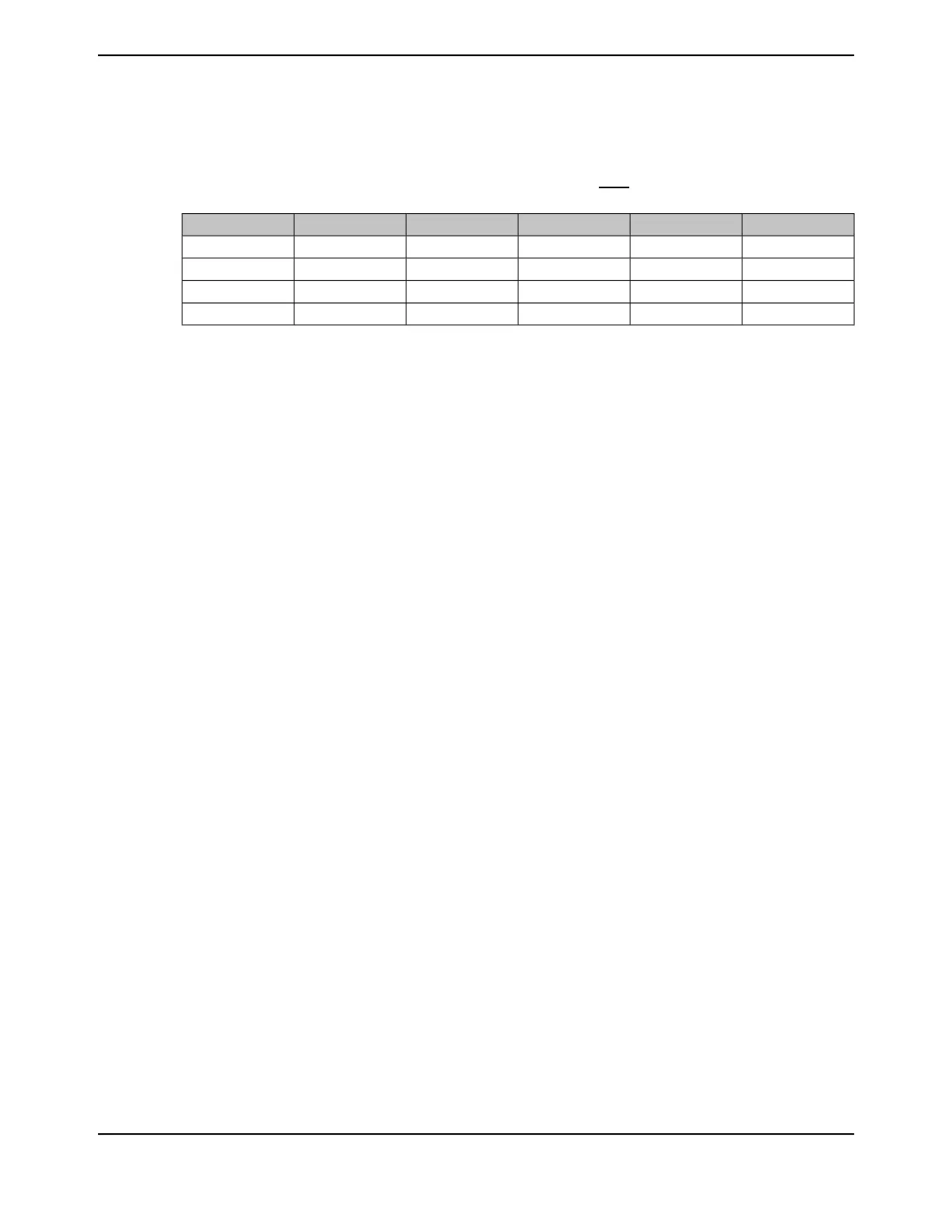
Table 4-2. JTAG Port Pins State after Power-On Reset or RST assertion
Drive ValueDrive StrengthInternal Pull-DownInternal Pull-UpData DirectionPin Name
N/AN/ADisabledEnabledInputTCK
N/AN/ADisabledEnabledInputTMS
N/AN/ADisabledEnabledInputTDI
High-Z2-mA driverDisabledEnabledOutputTDO
4.3.1.1 Test Clock Input (TCK)
The TCK pin is the clock for the JTAG module. This clock is provided so the test logic can operate
independently of any other system clocks and to ensure that multiple JTAG TAP controllers that
are daisy-chained together can synchronously communicate serial test data between components.
During normal operation, TCK is driven by a free-running clock with a nominal 50% duty cycle. When
necessary, TCK can be stopped at 0 or 1 for extended periods of time. While TCK is stopped at 0
or 1, the state of the TAP controller does not change and data in the JTAG Instruction and Data
Registers is not lost.
By default, the internal pull-up resistor on the TCK pin is enabled after reset, assuring that no clocking
occurs if the pin is not driven from an external source. The internal pull-up and pull-down resistors
can be turned off to save internal power as long as the TCK pin is constantly being driven by an
external source (see page 776 and page 778).
4.3.1.2 Test Mode Select (TMS)
The TMS pin selects the next state of the JTAG TAP controller. TMS is sampled on the rising edge
of TCK. Depending on the current TAP state and the sampled value of TMS, the next state may be
entered. Because the TMS pin is sampled on the rising edge of TCK, the IEEE Standard 1149.1
expects the value on TMS to change on the falling edge of TCK.
Holding TMS high for five consecutive TCK cycles drives the TAP controller state machine to the
Test-Logic-Reset state. When the TAP controller enters the Test-Logic-Reset state, the JTAG
module and associated registers are reset to their default values. This procedure should be performed
to initialize the JTAG controller. The JTAG Test Access Port state machine can be seen in its entirety
in Figure 4-2 on page 212.
By default, the internal pull-up resistor on the TMS pin is enabled after reset. Changes to the pull-up
resistor settings on GPIO Port C should ensure that the internal pull-up resistor remains enabled
on PC1/TMS; otherwise JTAG communication could be lost (see page 776).
4.3.1.3 Test Data Input (TDI)
The TDI pin provides a stream of serial information to the IR chain and the DR chains. TDI is
sampled on the rising edge of TCK and, depending on the current TAP state and the current
instruction, may present this data to the proper shift register chain. Because the TDI pin is sampled
on the rising edge of TCK, the IEEE Standard 1149.1 expects the value on TDI to change on the
falling edge of TCK.
By default, the internal pull-up resistor on the TDI pin is enabled after reset. Changes to the pull-up
resistor settings on GPIO Port C should ensure that the internal pull-up resistor remains enabled
on PC2/TDI; otherwise JTAG communication could be lost (see page 776).
June 18, 2014210
Texas Instruments-Production Data
JTAG Interface
 Loading...


