Table 18-1. I2C Signals (128TQFP) (continued)
DescriptionBuffer TypePin TypePin Mux / Pin
Assignment
Pin NumberPin Name
I
2
C module 8 clock. Note that this signal has an
active pull-up. The corresponding port pin should
not be configured as open drain.
ODI/OPD2 (2)
PA2 (2)
3
35
I2C8SCL
I
2
C module 8 data.ODI/OPD3 (2)
PA3 (2)
4
36
I2C8SDA
I
2
C module 9 clock. Note that this signal has an
active pull-up. The corresponding port pin should
not be configured as open drain.
ODI/OPA0 (2)33I2C9SCL
I
2
C module 9 data.ODI/OPA1 (2)34I2C9SDA
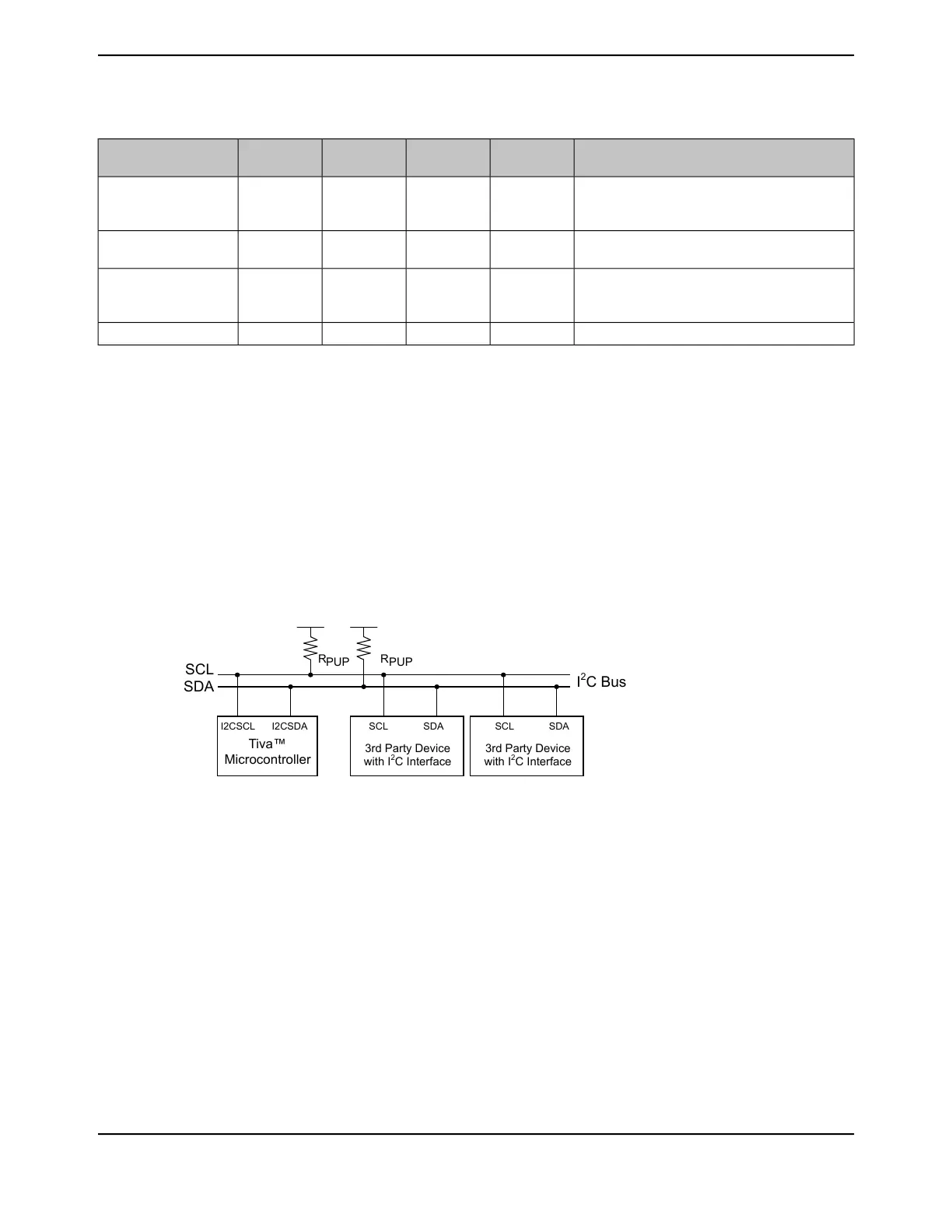
18.3 Functional Description
Each I
2
C module is comprised of both master and slave functions and is identified by a unique
address. A master-initiated communication generates the clock signal, SCL. For proper operation,
the SDA pin must be configured as an open-drain signal. Due to the internal circuitry that supports
high-speed operation, the SCL pin must not be configured as an open-drain signal, although the
internal circuitry causes it to act as if it were an open drain signal. Both SDA and SCL signals must
be connected to a positive supply voltage using a pull-up resistor. A typical I
2
C bus configuration is
shown in Figure 18-2. Refer to the I2C-bus specification and user manual to determine the size of
the pull-ups needed for proper operation.
See “Inter-Integrated Circuit (I
2
C) Interface” on page 1870 for I
2
C timing diagrams.
Figure 18-2. I
2
C Bus Configuration
R
PUP
Tiva™
Microcontroller
I2CSCL I2CSDA
R
PUP
3rd Party Device
with I
2
C Interface
SCL SDA
I
2
C Bus
SCL
SDA
SCL SDA
3rd Party Device
with I
2
C Interface
18.3.1 I
2
C Bus Functional Overview
The I
2
C bus uses only two signals: SDA and SCL, named I2CSDA and I2CSCL on TM4C1294NCPDT
microcontrollers. SDA is the bi-directional serial data line and SCL is the bi-directional serial clock
line. The bus is considered idle when both lines are High.
Every transaction on the I
2
C bus is nine bits long, consisting of eight data bits and a single
acknowledge bit. The number of bytes per transfer (defined as the time between a valid START
and STOP condition, described in “START and STOP Conditions” on page 1279) is unrestricted, but
each data byte has to be followed by an acknowledge bit, and data must be transferred MSB first.
When a receiver cannot receive another complete byte, it can hold the clock line SCL Low and force
the transmitter into a wait state. The data transfer continues when the receiver releases the clock
SCL.
June 18, 20141278
Texas Instruments-Production Data
Inter-Integrated Circuit (I
2
C) Interface
 Loading...


