Register 39: ADC Sample Sequence 1 Sample and Hold Time (ADCSSTSH1),
offset 0x07C
Register 40: ADC Sample Sequence 2 Sample and Hold Time (ADCSSTSH2),
offset 0x09C
These registers control the sample period size for each sample step of sequencer 1 and sequencer
2. Each sample and hold period select specifies the time allocated to the sample and hold circuit
as shown by the encodings in Table 15-3 on page 1058.
Note: If sampling the internal temperature sensor, the sample and hold width should be at least
16 ADC clocks (TSHn = 0x4).
Table 15-9. Sample and Hold Width in ADC Clocks
N
SH
TSHn Encoding
40x0
reserved0x1
80x2
reserved0x3
160x4
reserved0x5
320x6
reserved0x7
640x8
reserved0x9
1280xA
reserved0xB
2560xC
reserved0xD-0xF
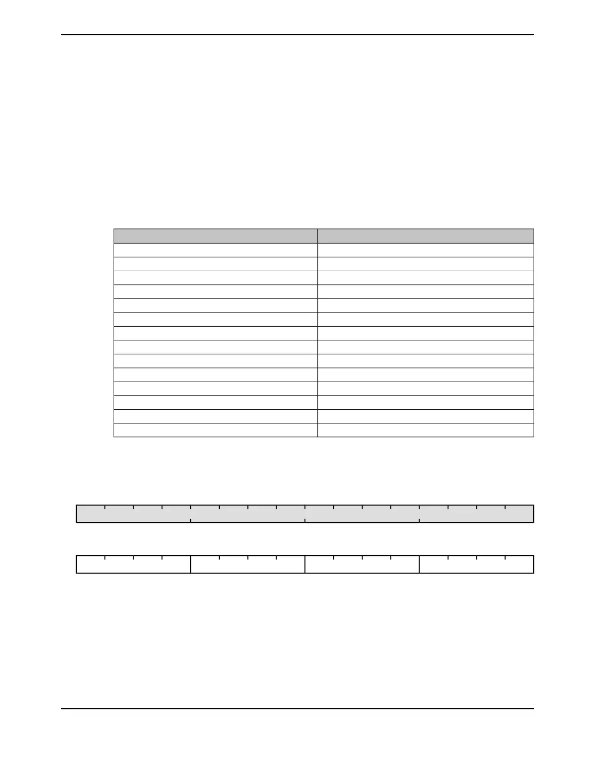
ADC Sample Sequence n Sample and Hold Time (ADCSSTSHn)
ADC0 base: 0x4003.8000
ADC1 base: 0x4003.9000
Offset 0x07C
Type RW, reset 0x0000.0000
16171819202122232425262728293031
reserved
ROROROROROROROROROROROROROROROROType
0000000000000000Reset
0123456789101112131415
TSH0TSH1TSH2TSH3
RWRWRWRWRWRWRWRWRWRWRWRWRWRWRWRWType
0000000000000000Reset
DescriptionResetTypeNameBit/Field
Software should not rely on the value of a reserved bit. To provide
compatibility with future products, the value of a reserved bit should be
preserved across a read-modify-write operation.
0x0000ROreserved31:16
1139June 18, 2014
Texas Instruments-Production Data
Tiva
™
TM4C1294NCPDT Microcontroller
 Loading...


