Register 15: Divisor and Source Clock Configuration (DIVSCLK), offset 0x148
The DIVSCLK register specifies the source and divisor of the DIVSCLK reference clock output. This
signal can be used as a clock source to an external device but bears no timing relationship to other
signals.
Note: The DIVSCLK signal output is not synchronized to the System Clock.
Divisor and Source Clock Configuration (DIVSCLK)
Base 0x400F.E000
Offset 0x148
Type RW, reset 0x0000.0000
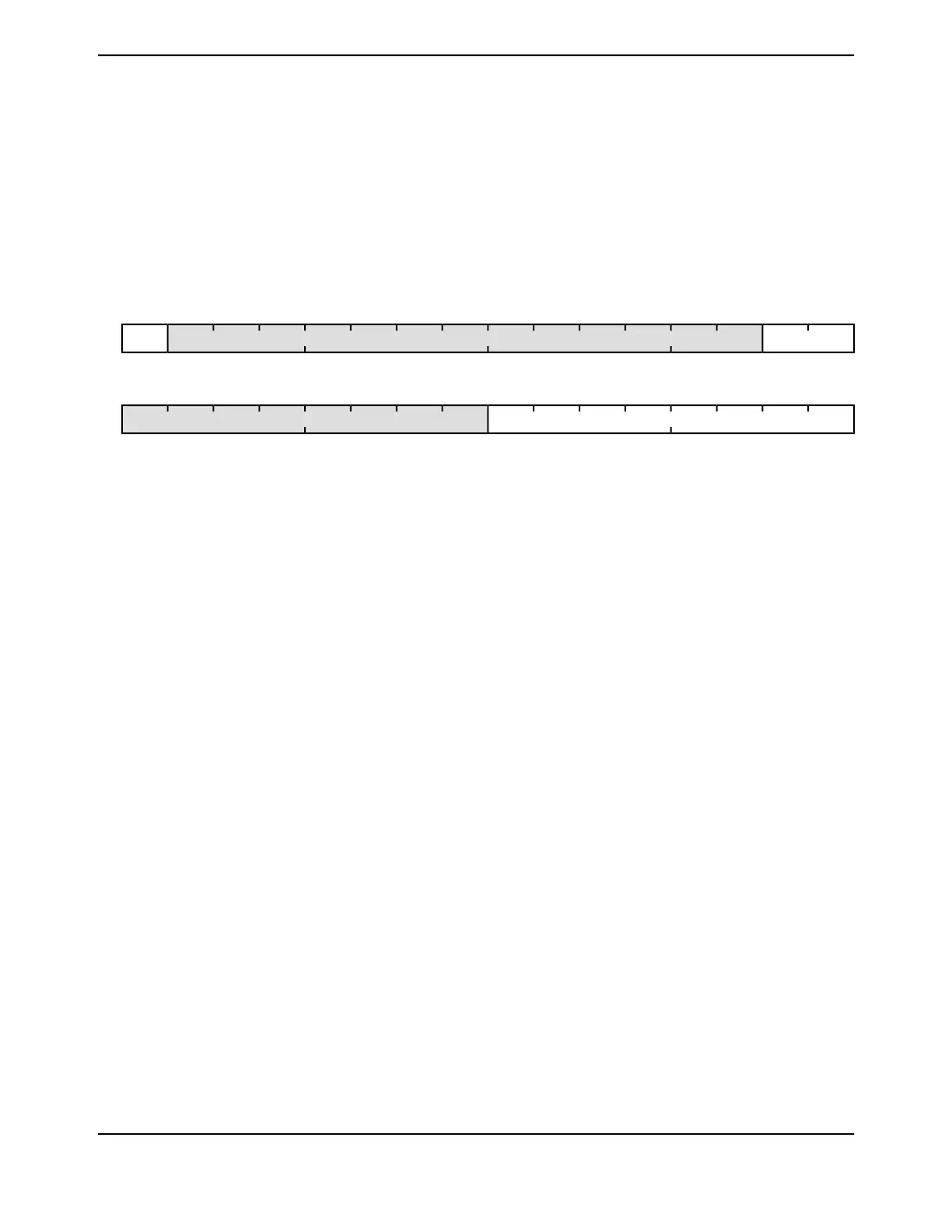
16171819202122232425262728293031
SRCreservedEN
RWRWRORORORORORORORORORORORORORWType
0000000000000000Reset
0123456789101112131415
DIVreserved
RWRWRWRWRWRWRWRWROROROROROROROROType
0000000000000000Reset
DescriptionResetTypeNameBit/Field
DIVSCLK Enable
This bit enables the generation of the DIVSCLK clock output. It resets
to 0 to disable the output thereby reducing initial current/power
consumption.
DescriptionValue
The clock output is disabled0
Clock output is enabled.1
0RWEN31
Software should not rely on the value of a reserved bit. To provide
compatibility with future products, the value of a reserved bit should be
preserved across a read-modify-write operation.
0ROreserved30:18
Clock Source
Selects the reference clock used to generate the output.
DescriptionValue
System Clock0x0
PIOSC0x1
MOSC0x2
reserved0x3
0RWSRC17:16
Software should not rely on the value of a reserved bit. To provide
compatibility with future products, the value of a reserved bit should be
preserved across a read-modify-write operation.
0ROreserved15:8
June 18, 2014284
Texas Instruments-Production Data
System Control
 Loading...


