Register 16: Flash DMA Starting Address (FLASHDMAST), offset 0xFD4
The starting address for the Flash region accessible by the µDMA is programmed in the
FLASHDMAST register.
Note: The µDMA can access Flash in Run Mode only (not available in low power modes).
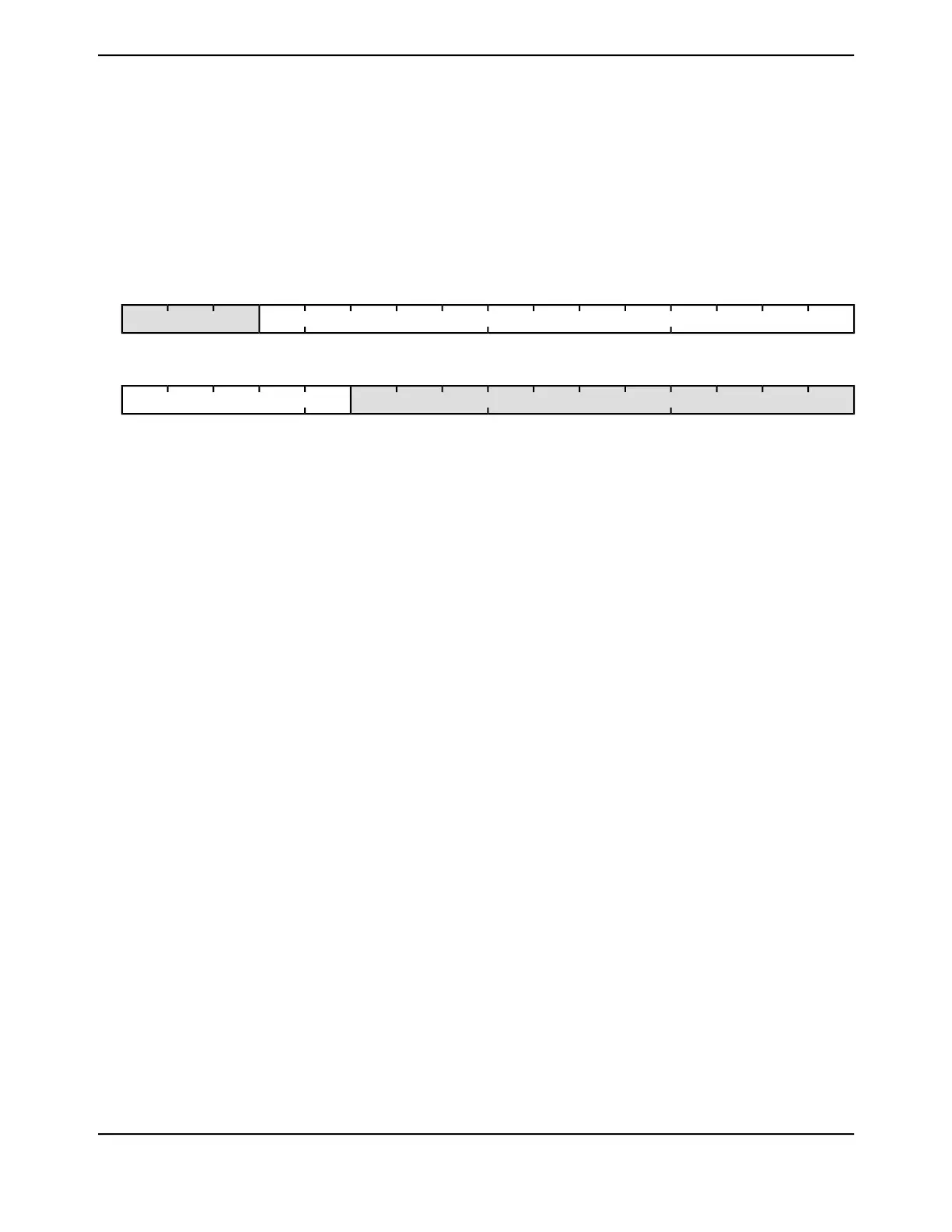
Flash DMA Starting Address (FLASHDMAST)
Base 0x400F.D000
Offset 0xFD4
Type RW, reset 0x0000.0000
16171819202122232425262728293031
ADDRreserved
RWRWRWRWRWRWRWRWRWRWRWRWRWROROROType
0000000000000000Reset
0123456789101112131415
reservedADDR
RORORORORORORORORORORORWRWRWRWRWType
0000000000000000Reset
DescriptionResetTypeNameBit/Field
Software should not rely on the value of a reserved bit. To provide
compatibility with future products, the value of a reserved bit should be
preserved across a read-modify-write operation.
0x0ROreserved31:29
Contains the starting address of the flash region accessible by µDMA
if the FLASHPP register DFA bit is set
0x0RWADDR28:11
Software should not rely on the value of a reserved bit. To provide
compatibility with future products, the value of a reserved bit should be
preserved across a read-modify-write operation.
0x0ROreserved10:0
8.5 EEPROM Register Descriptions (EEPROM Offset)
This section lists and describes the EEPROM registers, in numerical order by address offset.
Registers in this section are relative to the EEPROM base address of 0x400A.F000.
Note that the EEPROM module clock must be enabled before the registers can be programmed
(see page 400). There must be a delay of 3 system clocks after the EEPROM module clock is enabled
before any EEPROM module registers are accessed. In addition, after enabling or resetting the
EEPROM module, software must wait until the WORKING bit in the EEDONE register is clear before
accessing any EEPROM registers.
June 18, 2014650
Texas Instruments-Production Data
Internal Memory
 Loading...


