Register 10: Flash Write Buffer n (FWBn), offset 0x100 - 0x17C
These 32 registers hold the contents of the data to be written into the Flash memory on a buffered
Flash memory write operation. The offset selects one of the 32-bit registers. Only FWBn registers
that have been updated since the preceding buffered Flash memory write operation are written into
the Flash memory, so it is not necessary to write the entire bank of registers in order to write 1 or
2 words. The FWBn registers are written into the Flash memory with the FWB0 register corresponding
to the address contained in FMA. FWB1 is written to the address FMA+0x4 etc. Note that only data
bits that are 0 result in the Flash memory being modified. A data bit that is 1 leaves the content of
the Flash memory bit at its previous value.
Flash Write Buffer n (FWBn)
Base 0x400F.D000
Offset 0x100 - 0x17C
Type RW, reset 0x0000.0000
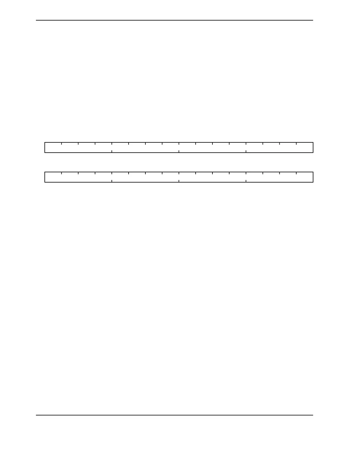
16171819202122232425262728293031
DATA
RWRWRWRWRWRWRWRWRWRWRWRWRWRWRWRWType
0000000000000000Reset
0123456789101112131415
DATA
RWRWRWRWRWRWRWRWRWRWRWRWRWRWRWRWType
0000000000000000Reset
DescriptionResetTypeNameBit/Field
Data
Data to be written into the Flash memory.
0x0000.0000RWDATA31:0
641June 18, 2014
Texas Instruments-Production Data
Tiva
™
TM4C1294NCPDT Microcontroller
 Loading...


