4. {00, 00, 00, D3}
5. {00, 00, 00, D4}
6. {00, 00, 00, D5}
7. {00, 00, 00, D6}
8. ......
9. .....
■ If operating in word mode, the CRCDIN register should be written in the following order:
1. {D3, D2, D1, D0}
2. {D7, D6, D5, D4}
3. {D11, D10, D9, D8}
4. ......
5. ......
12.3 Register Map
Table 12-3 on page 949 lists the CRC Module registers. The offset listed is a hexadecimal increment
to the register's address, relative to the base address 0x4403.0000.
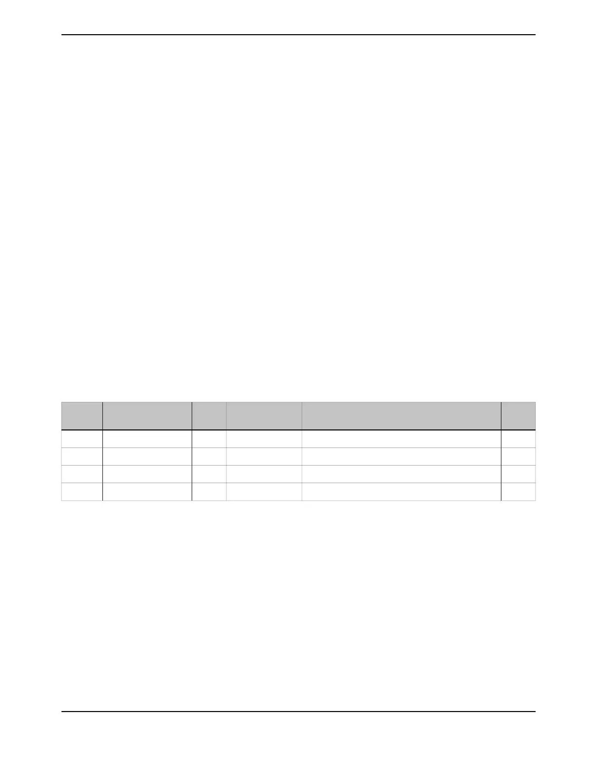
Table 12-3. CCM Register Map
See
page
DescriptionResetTypeNameOffset
950CRC Control0x0000.0000RWCRCCTRL0x400
952CRC SEED/Context0x0000.0000RWCRCSEED0x410
953CRC Data Input0x0000.0000RWCRCDIN0x414
954CRC Post Processing Result0x0000.0000ROCRCRSLTPP0x418
12.4 CRC Module Register Descriptions
This section lists and describes the CRC registers, in numerical order by address offset.
Note: The CRC module can only be accessed through privileged mode. If the µDMA is used for
CRC transfers, then the µDMA's DMA Channel Control (DMACHCTL) register also needs
to be programmed to allow for privileged accesses.
949June 18, 2014
Texas Instruments-Production Data
Tiva
™
TM4C1294NCPDT Microcontroller
 Loading...


