27.11 Hibernation Module
The Hibernation module requires special system implementation considerations because it is intended
to power down all other sections of its host device, refer to “Hibernation Module” on page 531.
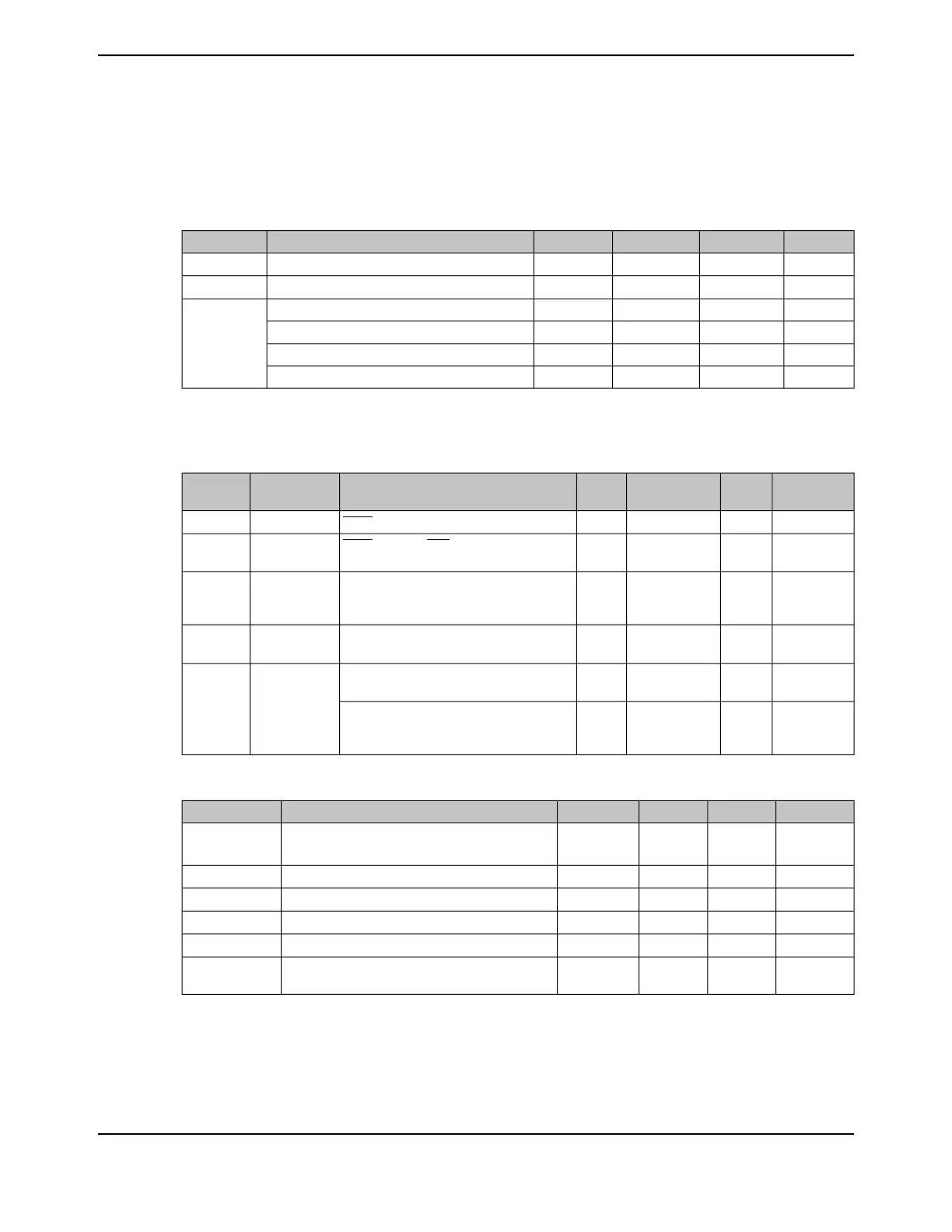
Table 27-29. Hibernation Module Battery Characteristics
UnitMaxNominalMinParameter NameParameter
V3.6
a
3.01.8Battery supply voltageV
BAT
V/µs0.7-0V
BAT
battery supply voltage ramp timeV
BATRMP
b
V2.01.91.8Low battery detect voltage, VBATSEL=0x0
V
LOWBAT
V2.22.12.0Low battery detect voltage, VBATSEL=0x1
V2.42.32.2Low battery detect voltage, VBATSEL=0x2
V2.62.52.4Low battery detect voltage, VBATSEL=0x3
a. To ensure proper functionality, any voltage input higher than V
BAT
Max, must be connected through a diode.
b. For recommended V
BAT
RC circuit values, refer to the diagrams located in“Hibernation Clock Source” on page 535.
Table 27-30. Hibernation Module Characteristics
UnitMaxNomMinParameter NameParameterParameter
No
ns--100WAKE assertion timeT
WAKE
H1
Hibernation
clock period
1--WAKE assert to HIB desassert (wake up
time)
T
WAKE_TO_HIB
H2
μs-Depends on
characteristics
of power supply
-V
DD
ramp to 3.0 VT
VDD_RAMP
H3
μs500--V
DD
at 3.0 V to internal POR deassert; first
instruction executes
T
VDD_CODE
H4
%60-40Duty cycle for RTCCLK output signal, when
using a 32.768-kHz crystal
DC
RTCCLK
H5
%70-30Duty cycle for RTCCLK output signal, when
using a 32.768-kHz external single-ended
(bypass) clock source
Table 27-31. Hibernation Module Tamper I/O Characteristics
UnitMaxNominalMinParameter NameParameter
MΩ5.2
-
4.43.5
-
TMPRn pull-up resistorR
TPU
µs--62TMPRn pulse width with short glitch filterT
SP
ms--94TMPRn pulse width with long glitch filterT
LP
µs95--TMPRn assertion to NMI (short glitch filter)T
NMIS
ms94--TMPRn assertion to NMI (long glitch filter)T
NMIL
V--V
BAT
*0.8TMPRn high-level input voltage when operating
from VBAT
V
IH
1845June 18, 2014
Texas Instruments-Production Data
Tiva
™
TM4C1294NCPDT Microcontroller
 Loading...


