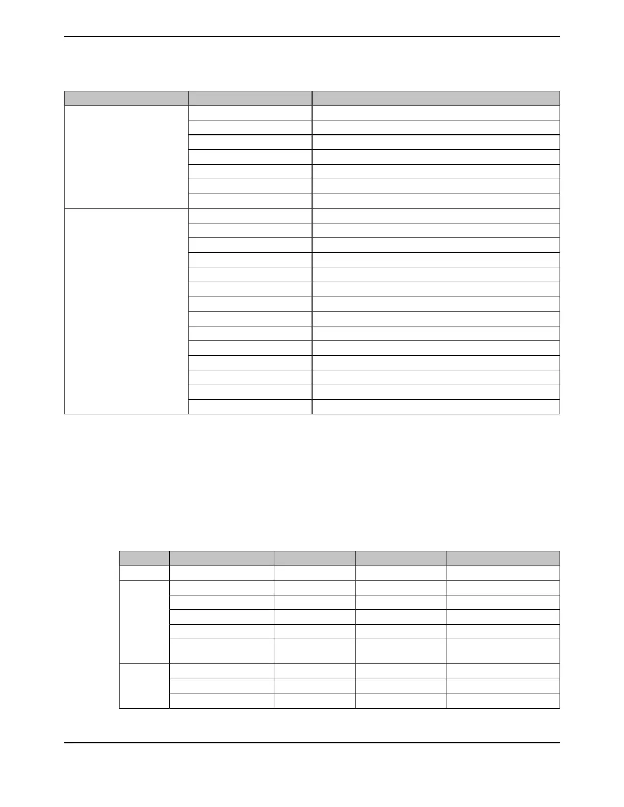
Table 26-6. Possible Pin Assignments for Alternate Functions (continued)
GPIO FunctionAlternate Function# of Possible Assignments
U3CTS PN5 PP5
PN4 PP4U3RTS
PA4 PJ0U3Rx
PA5 PJ1U3Tx
PA2 PK0U4Rx
PA3 PK1U4Tx
PA7 PD7USB0PFLT
PL1 PN5 PP5I2C2SCL
three
PC5 PK7 PP3RTCCLK
PA0 PD0 PL4T0CCP0
PA1 PD1 PL5T0CCP1
PA2 PD2 PL6T1CCP0
PA3 PD3 PL7T1CCP1
PA6 PD4 PM2T3CCP0
PA7 PD5 PM3T3CCP1
PB0 PD6 PM4T4CCP0
PB1 PD7 PM5T4CCP1
PB4 PH1 PM4U0CTS
PH2 PM5 PP3U0DCD
PH3 PM6 PP4U0DSR
PA6 PA7 PD6USB0EPEN
26.6 Connections for Unused Signals
Table 26-7 on page 1816 shows how to handle signals for functions that are not used in a particular
system implementation for devices that are in a 128-pin TQFP package. Two options are shown in
the table: an acceptable practice and a preferred practice for reduced power consumption and
improved EMC characteristics. If a module is not used in a system, and its inputs are grounded, it
is important that the clock to the module is never enabled by setting the corresponding bit in the
RCGCx register.
Table 26-7. Connections for Unused Signals (128-Pin TQFP)
Preferred PracticeAcceptable PracticePin NumberSignal NameFunction
VDDAVDDA9VREFA+ADC
NCNC53EN0RXIN
Ethernet
NCNC54EN0RXIP
NCNC56EN0TXON
NCNC57EN0TXOP
NC
a
Connect to ground
through 4.87K resistor
59RBIAS
GND
b
NC34PA1(UART0TX)
GPIO GND
c
NC37PA4 (SSI0XDAT0)
GNDNC-All unused GPIOs
June 18, 20141816
Texas Instruments-Production Data
Signal Tables
 Loading...


